Sn-Pb EMI Filter & Decoupling Capacitors
EMI filter capacitors employ a unique, patented low inductance design featuring two balanced capacitors that are immune to temperature, voltage and aging performance differences. These components offer superior decoupling and EMI filtering performance, virtually eliminate parasitics, and can replace multiple capacitors and inductors saving board space and reducing assembly costs.

Advantages:
- One device for EMI suppression or decoupling
- Replace up to 7 components with one EMI
- Differential and common mode attenuation
- Matched capacitance line to ground, both lines
- Low inductance due to cancellation effect
Applications:
- Amplifier Filter & Decoupling
- High Speed Data Filtering
- EMC I/O Filtering
- FPGA / ASIC / μ-P Decoupling
- DDR Memory Decoupling
Technical Notes:
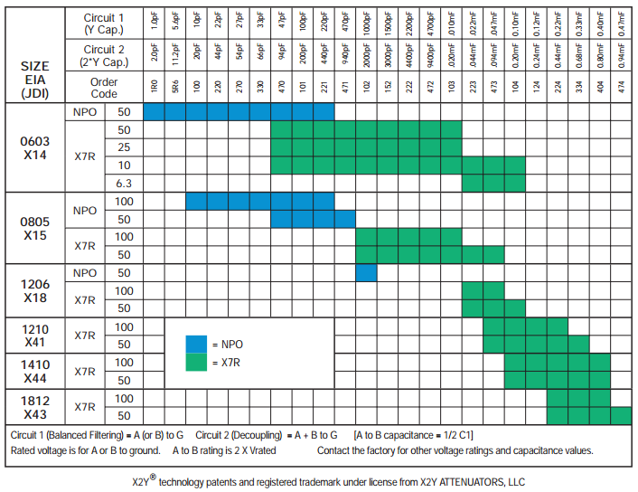
Capacitance Selection
Electrical Characteristics
EMI Filtering Scc21
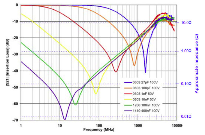
Power Bypass S21
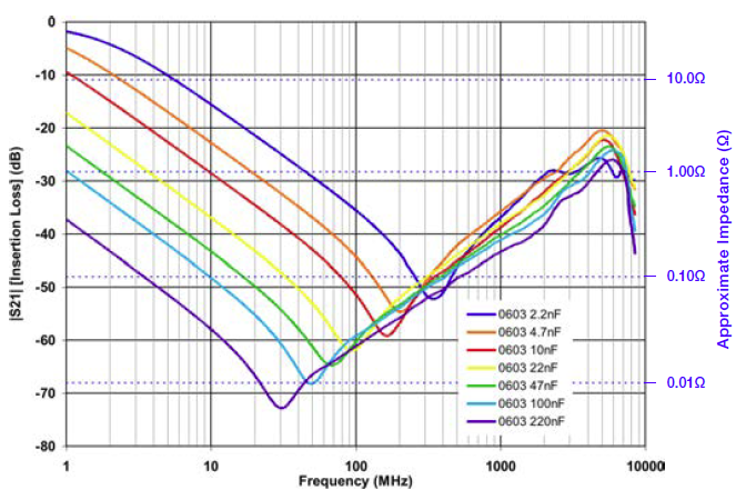
More data at S21 Plotter
Mechanical Specifications
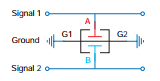
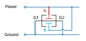
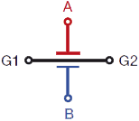
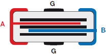
Equivalent Circuits
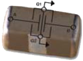
Cross Sectional View
Dimensional View

Mechanical Specifications
| 0402 (X07) | 0603 (X14) | 0805 (X15) | 1206 (X18) | 1210 (X41) | 1410 (X44) | 1812 (X43) | ||||||||
|---|---|---|---|---|---|---|---|---|---|---|---|---|---|---|
| IN | mm | IN | mm | IN | mm | IN | mm | IN | mm | IN | mm | IN | mm | |
| L | 0.045 ± 0.003 | 1.143 ± 0.076 | 0.064 ± 0.005 | 1.626 ± 0.127 | 0.080 ± 0.008 | 2.032 ± 0.203 | 0.124 ± 0.010 | 3.150 ± 0.254 | 0.125 ± 0.010 | 3.175 ± 0.254 | 0.140 ± 0.010 | 3.556 ± 0.254 | 0.174 ± 0.010 | 4.420 ± 0.254 |
| W | 0.024 ± 0.003 | 0.610 ± 0.076 | 0.035 ± 0.005 | 0.889 ± 0.127 | 0.050 ± 0.008 | 1.270 ± 0.203 | 0.063 ± 0.010 | 1.600 ± 0.254 | 0.098 ± 0.010 | 2.489 ± 0.254 | 0.098 ± 0.010 | 2.490 ± 0.254 | 0.125 ± 0.010 | 3.175 ± 0.254 |
| T | 0.020 max | 0.508 max | 0.026 max | 0.660 max | 0.040 max | 1.016 max | 0.050 max | 1.270 max | 0.070 max | 1.778 max | 0.070 max | 1.778 max | 00.090 max | 2.286 max |
| EB | 0.008 ± 0.003 | 0.203 ± 0.076 | 0.009 ± 0.005 | 0.229 ± 0.127 | 0.009 ± 0.004 | 0.229 ± 0.102 | 0.009 ± 0.004 | 0.229 ± 0.102 | 0.009 ± 0.005 | 0.229 ± 0.127 | 0.009 ± 0.005 | 0.229 ± 0.127 | 0.009 ± 0.005 | 0.229 ± 0.127 |
| CB | 0.010 ± 0.003 | 0.305 ± 0.076 | 0.0018 ± 0.005 | 0.457 ± 0.127 | 0.022 ± 0.005 | 0.559 ± 0.127 | 0.040 ± 0.005 | 1.016 ± 0.127 | 0.045 ± 0.005 | 1.143 ± 0.127 | 0.045 ± 0.005 | 1.143 ± 0.127 | 0.045 ± 0.005 | 1.143 ± 0.127 |
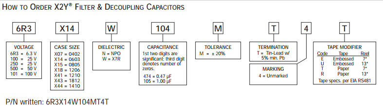
How to Order