Sn/Pb SMT Application Notes
General
Soldering temperature profiles used must provide adequatetemperature rise time and cool-down time to prevent damagedue to thermal shock. These guidelines are emphasized becausecracking or other damage caused by handling or thermal shockis not necessarily apparent under ordinary visual inspectiontechniques. The damage can be very small (micro-cracks) andcan occur under the terminations where even high magnificationcannot detect them. The problem is further complicated bythe fact that these micro-cracks may not be initially detectableby standard electrical testing. Once initiated, the cracks cangrow with time and cause latent failures. Attention to thesedetails will aid in the successful use of the inherently reliablemultilayer ceramic capacitor.
Ceramic capacitors larger then EIA size 1812 are known to bevery susceptible to thermal shock damage due to their largeceramic mass. These large parts require more care during installationthan smaller surface mount devices.
SOLDER PRE-HEAT CYCLE
Proper preheating is essential to prevent thermal shock crackingof the capacitor. The circuit assembly should be preheated asshown in the recommended profiles at a rate of 1.0 to 2.0°C persecond to within approximately 100°C of the maximum solderingtemperature. Temperature change should be distributed asevenly as possible throughout large capacitor bodies as applyingheat or cold to a localized spot on the device may result inthermal gradients great enough to cause cracking.
SMT SOLDERING TEMPERATURES
Solders typically utilized in SMT have melting points between179°C and 188°C. Activation of rosin fluxes occurs at about200°C. Based on these parameters, typical maximum reflowtemperatures run between 210 to 230°C. Use of thermal profilingis advised for accurate characterization of circuit heatabsorption and maximum component temperature conditionsthat occur during the soldering process.
SOLDER REFLOW
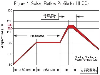
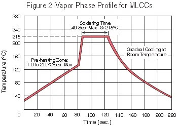
Recommended temperature profiles for reflow soldering areshown in Figures 1 & 2. A maximum heating rate of 3°C/sec.(4°C/sec. for vapor phase) should not be exceeded between thepre-heat cycle and maximum soldering temperature.
SOLDER WAVE
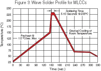
Wave soldering can be utilized, but the preheat requirementsgenerally make this process very difficult to accomplish. Recommendedtemperature profile for wave soldering is shown inFigure 3. Wave soldering is not recommended for ceramic MLCCs larger then 1210 size due to the incompatibility ofthe chip's mass with the steep temperature gradient typicallypresent in this process.
Soldering Iron
Ceramic capacitor attachment with a soldering iron is d-iscouraged due to the inherent process control limitations. Inthe event that a soldering iron must be employed the -following precautions are recommended.
- Preheat circuit and capacitors to 150°C
- Never contact the capacitor with the iron tip
- 30 watt iron output (max)
- 280°C tip temperature (max)
- 3.0 mm tip diameter (max)
- Limit soldering time to 5 sec.
IPC 7351 Land Pattern Guidelines
Appropriate pad design, solder application, and component orientation are all ingredients of a quality, defect-free soldering process. TheInstitute for Interconnecting and Packaging Electronic Circuits (IPC)has developed and published IPC 7351 "Surface Mount Design andLand Pattern Standard". This standard presents industry consensus on optimum dimensions based on empirical knowledge of fabricated landpatterns. The standard also contains an excellent analysis of solderjoints and their relation to component, PCB, and placement tolerances.A summary of the IPC land pattern design recommendations for solderreflow and solder wave processes are listed in table below. It is highlyrecommended that the PCB designer/SMT process engineer obtain thecomplete IPC 7351 standard (
)
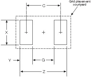
| Chip EIA | Size (mm) | Reflow Solder | Solder Wave | ||||||||
|---|---|---|---|---|---|---|---|---|---|---|---|
| Z | G | X | Y(ref) | C(ref) | Z | G | X | Y(ref) | C(ref) | ||
| 0402 | 1005 | 2.4 | 0.4 | 1.3 | 1.0 | 1.4 | |||||
| 0603 | 1608 | 2.8 | 0.6 | 1.0 | 1.1 | 1.7 | 3.18 | 0.68 | 0.80 | 1.25 | 1.93 |
| 0805 | 2012 | 3.2 | 0.6 | 1.5 | 1.3 | 1.9 | 3.70 | 0.70 | 1.10 | 1.50 | 2.20 |
| 1206 | 3216 | 4.4 | 1.2 | 2.7 | 1.6 | 2.8 | 4.90 | 1.50 | 1.40 | 1.70 | 3.20 |
| 1210 | 3225 | 4.4 | 1.2 | 2.7 | 1.6 | 2.8 | 4.90 | 1.50 | 2.00 | 1.70 | 3.20 |
| 1808 | 4520 | 5.8 | 2.5 | 2.7 | 1.7 | 4.2 | Not Recommended | ||||
| 1812 | 4532 | 5.8 | 2.0 | 3.4 | 1.9 | 3.9 | |||||
| 1825 | 4564 | 5.8 | 2.0 | 6.8 | 1.9 | 3.9 | |||||
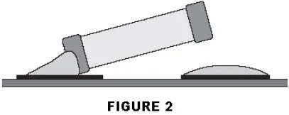
Tomb Stoning / Chip Movement
Tome-stoning or draw bridging is illustrated in figure 1.Tomb-stoning or other undesirable chip movements mayresult if unequal surface tension forces exist as the moltensolder wets the MLCC terminations and mounting pads.This tendency can be minimized by insuring that all factorsat both solder joints are equal, namely; pad size, soldermass, termination size, component position and heatingTomb-stoning is easily avoided through proper design,material selection and proofing of the process.