Arc Season & Board Design Observations
This year's arcing season is just now fading into bad memories as another year is past butknowing that a new season is just a Monsoon away. ARC season is well known to highvoltage capacitor vendors and users alike and with the drive to smaller high voltage (HV)components like ceramic capacitors we know that the next season will arrive sooner andlast longer. From a vendor’s standpoint parts are shipped that meet the publishedspecifications but when the customer mounts those same capacitors on an assembly, highvoltage problems can arise. There may be interactions between the board and fluxresidue, humidity absorption of both the PWB (Printed Wiring Board) and flux residue,what type of flux is used in the solder paste and the high voltage capability of the boarditself. These are the areas that need to be investigated.
Field Problems
Problems include test equipment correlation problems, test methods used for HV testing,but the big source of defects appear to be from a combination of the board layout,assembly pr°Cess, choice of solder paste flux and cleaning where required. A largenumber of contract manufacturers around the world use water soluble flux solder pastebecause it is much more aggressive that No-Clean flux allowing for wider reflow pr°Cesswindows and minimizes component solderability problems. Unfortunately organic acidsused in water soluble solder paste are very active and if the assembly is not adequatelycleaned those flux residues start their damage and are difficult to remove. Now we arefaced with high leakage currents, low arc voltages and assembly failures. Add humidityand we have a new ARC season. An interesting ARC season failure is shown in Figure 1.The board was reflow soldered using water soluble solder paste but not completelycleaned. The board design used a 2mm slot beneath 1808 case size high voltage safetycapacitors. The use of slots are a typical high voltage board design technique. Completeand thorough cleaning of all flux residues is mandatory when this design technique isused with water soluble flux. There were droplets of flux residue on the assembly bottomand visible flux residues on the bottom of all 1808 size safety capacitors. The burned arcpath shown in Figure 1 is along the slot edge in the PWB following flux residues.

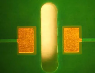
a) Flux Residues on Chip & PWB Bottom

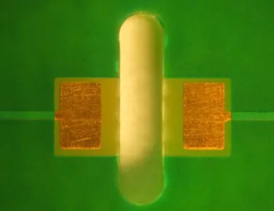
b) ARC Path in PWB Slot
Figure 1. Field Failure Due to Water Soluble Flux Residue
The Experiment
High voltage 1206 3kV 120pF X7R capacitors were mounted on boards with 4 variationsof pad/solder mask/slots to evaluate the impact common board layout techniques on ACbreakdown voltage. A 5 mil thick stencil was used to replicate the customer environment.Stencil apertures were 95% of the pad area. No-Clean and water soluble solder pasteformulations were evaluated to determine the interaction between flux and board layoutafter reflow soldering and after humidity exposure. An exposure time of 48 hours at85°C / 85% RH was chosen to drive moisture into the board and flux residues trappedbeneath the chips. The capacitors were not biased consistent with most high voltageisolation applications typical for smaller safety capacitors.
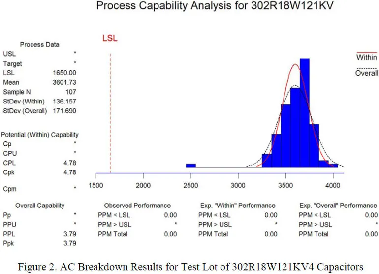
These capacitors chosen for this experiment are 1206 case size X7R 120pF and aredesigned for 1500VAC withstanding voltage commonly found in larger safety capacitors.A 107 piece sample of these parts was tested to AC breakdown with the results shown in Figure 1.
Board layout variations included solder mask between pads, no solder mask betweenpads, solder mask with a 0.040" (1mm) wide slot between pads and no solder mask witha 0.040" slot between pads. A larger slot was not practical for 1206 sized capacitorsbecause of pad to pad spacing of 0.080" (2mm) was used. Figure 3 shows each layoutvariation for reference. Removing solder mask from between pads allows solvent accessduring cleaning when water soluble flux is used and minimizes flux flow between thecapacitor pads due to capillary forces during reflow soldering.
Square pads were used as they are most commonly encountered on end customer'sboards. Additionally square pads are the easiest to draw in board layout programs. Eachevaluation board had 80 positions for each pad/solder mask/slot variation for increasedconfidence levels in the results. Bare board arcs were from pad corner to opposing padcorner as expected as square pad corners will have the highest electric field gradients.

a) Solder Mask between Pads
b) Solder Mask & Slot between Pads

c) No Solder Mask between Pads
d) No Solder Mask but Slot between Pads
Figure 3. Evaluation Board SMT Pad Variations
Two different solder paste and flux chemistries were used in these experiments and arelisted in Table 1. These were chosen as they were readily available and are typical ofsolder pastes commonly used during board assembly.
Table 1. Solder Paste Used in Experiments
| Paste Description | Type of Paste |
|---|---|
| ROL0 ANSI/J-STD-004 | No-Clean |
| ORH0 ANSI/J-STD-004 | Water Soluble |
The experimental procedure consisted of exposing both bare boards and assemblies toAC breakdown. A bare board as received was tested for AC breakdown voltagedistribution. A second evaluation board had Sn63 No-Clean solder paste stenciled on thepads and reflowed. Those results are listed in Appendix 1 and are used as a baseline forcomparisons with capacitors mounted to boards with different fluxes and humidityexposure. What is interesting is that the board AC breakdown capability significantlyincreased after exposure to reflow soldering temperatures. After components weresoldered to the boards and exposed to 48 hours of 85°C/85%RH those breakdownvoltages returned to values consistent with the bare board in an as received condition.Real world assemblies will absorb moisture after soldering and depending on where theassemblies are manufactured, stored and the 48 hours of humidity exposure the resultsinline with the board in its as received condition. The data for the bare board and thosewith capacitors solder to it is consistent with reflow soldering drying out the assembly.
Appendix 2 lists AC breakdown results for capacitors reflow soldered to an evaluationboard with No-Clean solder paste, tested approximately 18 hours after reflow solderingand an assembly that was exposed to 85°C at 85% RH for 48 hours and then tested 1 hourafter the board was removed from humidity exposure. Appendix 3 has assembled boardbreakdown results approximately after two hours after cleaning. This assembly usedwater soluble solder paste. The other breakdown data is for an assembly with capacitorsand water soluble solder paste, reflow soldered, cleaned and exposed to 85°C/85% RHfor 48 hours. This assembly was tested to breakdown within 2 hours of humidityexposure. Table 2 is a summary all of the AC breakdown results shown in theappendices.
Table 2. Summary of all Breakdown Test Mean Value Results (Volts)
| Pad Layout | Bare Bd. | NC Bd. | NC Caps | NC 85/85 | WS Caps | WS 8585 |
|---|---|---|---|---|---|---|
| Solder Mask | 2552 | 2952 | 3002 | 2682* | 2522 | 2327 |
| SM/Slot | 2615 | 3341 | 3075 | 3099 | 2622 | 2515 |
| No SM | 2406 | 3098 | 3097 | 2957 | 2624 | 2487 |
| No SM/Slot | 2619 | 3254 | 3150 | 3222 | 2859 | 2756 |
| Bare Bd. | Bare board as received |
| NC Bd. | Bare board reflow soldered with No-Clean solder paste |
| NC Caps | Board w/capacitors reflowed w/No-Clean solder paste |
| NC 85/85 | No-Clean solder paste w/caps after 48 hour exposure to 85°C/85%RH |
| WS Caps | Board w/capacitors reflowed w/water soluble solder paste |
| WS 85/85 | Water soluble solder paste w/caps after 48 hours of 85°C/85%RH |
* There were some breakdown values below the specification limit of 1500VAC and broad distribution of breakdown voltages
Observations
Examining both the mean of the breakdown voltages and the actual distributions shownin Appendices 2 and 3 are revealing. Solder mask between pads was consistently thepoorest performer in AC breakdown testing in these experiments. Slots between padswere consistently the best performers as expected. No solder mask between pads wascomparable with the layout option of solder mask and a slot between the capacitor pads.Figures 4 and 5 are the distributions for No-Clean solder paste with no solder maskbetween pads and water soluble solder paste with solder mask between pads with a0.040” (1mm) slot. Both assemblies underwent 48 hours exposure at 85°C/85%RH.


PWB Layout Suggestions
The data are consistent with eliminating high voltage slots where allowed and removal ofsolder mask between pads. Figure 6 represents a chip soldered to pads with and withoutsolder mask showing the added gap between chip bottom and PWB surface.

Flux residues are trapped between capacitor bodies and solder mask during reflowsoldering when the flux is liquid. This is due to capillary forces wicking the flux betweenthe solder mask and capacitor body. Figure 7 shows three parts removed from a boardthat suffered ARC season defects. The flux is clearly visible in this photo. The parts wereremoved by placing the assembly on a hot plate and were plucked off using tweezerswhen the solder reflowed. These particular boards had a 2mm slot between pads butfailed 1500VAC during HiPot testing. Bottom side of capacitors showing flux residuestrapped between capacitor bodies and solder mask. The flux flow stopped at the PWBslot and has arrows pointing to the flux gaps.

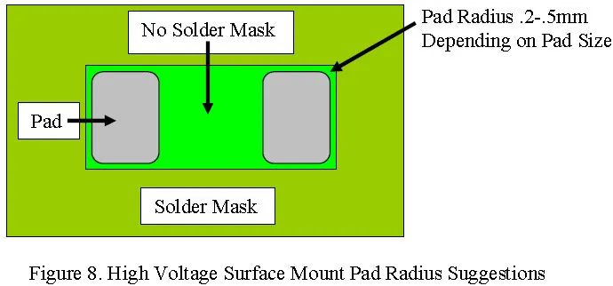
In addition to eliminating solder mask between pads, the pads themselves should haveradiuses instead of rectangular corners. All arcs emanated from pad corners due to thoselocations having the highest electric field gradients when exposed to high voltage fields.Adding a radius at each corner will reduce field gradients aid in high voltageperformance. Suggested pad radiuses are shown in Figure 8.
Summary
The data are consistent with cost savings by eliminating slots where possible byeliminating solder mask between pads. There is the additional benefit of creating cleaningaccess if water soluble solder paste is used in board assembly. And finally spreading outfield gradients by adding a radius to pads can aid in improving AC breakdownperformance. Each layout suggestion needs to be evaluated in new designs as each designwill have unknown quirks.
As a side note high voltage components should never have traces beneath the componentbody and voltage creepage requirements to eliminate arcing to adjacent components andtraces.
Notice:
Specifications are subject to change without notice. Contact your nearest Johanson Dielectrics Sales Office for the latest specifications. All statements, information and data given herein are believed to be accurate and reliable, but are presented without guarantee, warranty, or responsibility of any kind, expressed or implied. Statements or suggestions concerning possible use of our products are made without representation or warranty that any such use is free of patent infringement and are not recommendations to infringe any patents. The user should not assume that all safety measures are indicated or that other measures may not be required. Specifications are typical and may not apply to all applications.