Corona Effects and Their Impact on PWB Layout Induced HiPot Failures
John Maxwell Director of Product Development - Feb. 27, 2006Background
Understanding conorna interactions between PWB and components is essential to design board layouts that are robust with minimum corona related failures during HiPot testing and operation in a system. Understanding high voltage physics becomes important in understanding root cause of failure and effective corrective action when failures occur. Most research effort in the area of corona discharge has been performed in the high voltage power transmission industry. Dielectric or insulator degradation results when arcing occurs during corona dischage resulting in failure. Repeated corona or partial discharges can lead to dielectric or insulator wear out and eventual material failure making understanding the phenemona critical in designing high reliability systems.
Definition of Terms
- Ceramic: Metal oxide compounds
- Corona Inseption Voltage or CIV: The voltage where arcing occurs
- Dielectric: A non conducting material used to constrain the electric field and to provide charge storage.
- Dielectric Strength: The rupture voltage where thermal electrons within the material gain enough energy in the electric field to generate many more additional electrons through impact with atoms within the material. The current avalanches at this voltage.
- Ionized Gas: Molecules where elecgtrons have become stripped from the atoms
- ε Relative dielectric constant
- ε air 1
- ε dielectric Approximately 4-5
- ε capacitor Typically > 2000 for X7R Dielectrics
- Partial Discharge: Corona discharge within a dielectric material or structure
- Paschen's Minimum: the minimum corona inception voltage (CIV) between two closely spaced conductors separated by dielectric and is approximately 330V at 1 atmosphere in air.
- Quench Voltage: The voltage where arcing is extinguished, less than Paschen's Minimum voltage.
- Pseudo or Phantom Electrode: A dielectric structure that acts like a metallic electrode due to either shape, high dielectric constant or both
- Streamer Discharge: A long duration (>100nS) characterized by large discharge area and high charge transfer (>120pC at CIV).
- Townsend Discharge: Short duration (<10nS) characterized by small area and low charge transfer (<100pC at CIV).
PWB Considerations
The primary consideration in PWB (Printed Wiring Board) design is establishing acceptable spacing or creepage to meet regulatory requirements and is usually limited to conductor spacing on a board surface. Problems arise though when components are placed over those conductors during assembly. Dielectric constant of and spacing between dielectric layers of solder mask, flux residue, air and conductors all come into play when we evaluate corona events during HiPot testing. Figure 1 shows a typical layout that causes problems during HiPot testing. This is a two dimensional representation of a more complex three-dimensional problem.
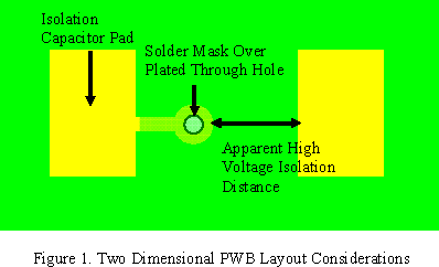
Figure 2 shows the relationship between isolation capacitor, capacitor pads and plated through hole via to inner layers of the PWB. This is were problems arise because the capacitor's high dielectric constant causes the ceramic dielectric body appear to be a pseudo or phantom electrode greatly reducing the high voltage isolation distance. In this case we now depend the rupture voltage properties of the solder mask to provide isolation between the capacitor body and opposing pad. Solder mask is specifically not designated as a dielectric material and designers cannot depend on solder mask providing high voltage isolation.
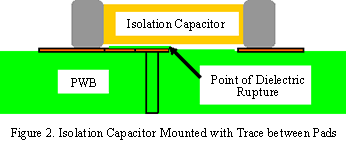
The capacitor is coupled to the copper trace on one side with the capacitor body acting as the opposing pseudo electrode on the other. Now solder mask thickness only isolates high voltages encountered during operation or HiPot testing. Voltage across those coupling capacitors is a function of capacitor area, dielectric constant, spacing and applied voltage. A voltage divider network is formed between pad and pseudo electrode. Figure 3 shows the relationship between pad, solder mask, spacing between capacitor body and pad. Figure 4 is of the coupling capacitors between pad and capacitor body pseudo electrode.
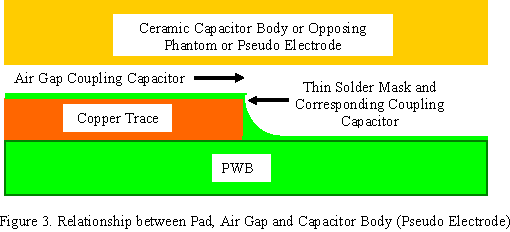
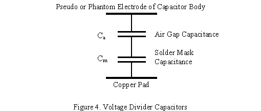
Problems begin when two conditions are present, thin solder mask coverage over the pad edge and when the voltage across the air gap between solder mask and capacitor body pseudo electrode exceeds Paschen's minimum. The low dielectric constant of air results in most of the applied voltage being dropped that capacitor Ca and a smaller voltage being dropped across the solder mask capacitor Cm. At that voltage Townsend partial discharges will occur across that air gap. During discharge the voltage across the air gap capacitor collapses due to air ionizing resulting in the entire applied voltage being across the solder mask dielectric. This can easily exceed the rupture voltage of this material resulting in a direct high voltage short. If any pad metallization becomes exposed due to Townsend partial discharges then a much larger streamer discharge occurs creating a volume of ionized gas trapped between the capacitor body and PWB surface. This trapped ionized gas supports current conduction and depending on the distance between where the first discharges occurred and opposing isolation capacitor pad the arc may extinguish or jump to that opposing pad on the PWB. Available charge, quench voltage, capacitor surface chemistry and physical distance to the opposing pads are factors that determine if the arc will reach to the opposing pad.
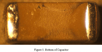
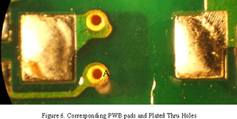
An example of this type of failure is shown in Figures 5 and 6. Both the capacitor bottom and PWB surface are shown. The point of arc inception (A) is clearly visible in both photos.
Ceramic capacitors are made with sintered grains or crystals on metal oxides. These ceramic dielectric materials are not insulators but polycrystalline semiconductor materials with nonlinear voltage current relationships. The presence of these metal crystals, surface smoothness, dielectric constant and air or ionizing gas practically limits the physical size of high voltage isolation capacitors. Typical safety capacitors are case size 1808 or 180 mils long and 80 mils wide to meet these high voltage creepage distances.
Conclusions
Two-dimensional PWB layout techniques cannot be used when ceramic isolation capacitors are used. No trace or plated through holes can be placed between those isolation capacitor pads for the reasons discussed. We have to evaluate and understand the impact of adding a high k dielectric layer directly over any trace or pad and how it dramatically reduces isolation distances by acting as a pseudo electrode.


