Amplifier Decoupling: EMI vs MLCC
EMI Amplifier Decoupling
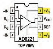
Test #1
- Uses an AD8221 instrumentation amplifier
- Pin pattern is amenable to EMI circuit 1” use
- +V / -V power pins are on the same side of the device

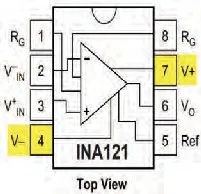
Test #2
- Uses an INA121 instrumentation amplifier
- Pin pattern is amenable to EMI”circuit 2” use
- +V / -V power pins are on the opposite sides of the device
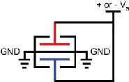
Compare Bypass Conventional MLCC vs. EMI
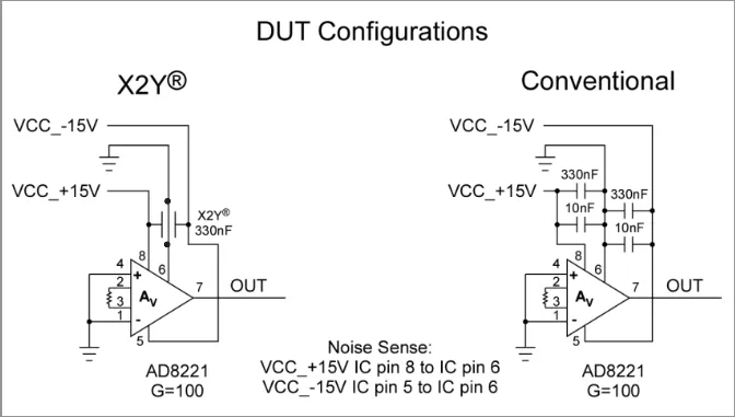
Test #1
- Compares external noise rejection of power bypass networks
– Single EMI 330nF rated part, versus four total MLCCs - Noise voltage measured directly across IC pins
PCB Configuration
Test #1
- Two layer 1.5mm PCB
- Single EMI 330nF rated part, versus four total MLCCs
- Noise voltage probed directly across IC pins at IC body

PCB Configuration
Test #1
- Equalized layout parasitics
- Ground attachment matched between set-ups
- Capacitor set-backs matched between set-ups

Noise Injection
- 200ps edges
– Comparable to memory - 100MHz pulse rate
– Isolate any cavity / capacitor ringing - 400mV on 15V power
– Alternate tests:
+15V / -15V - – 2.7% pp


VCC_15V+
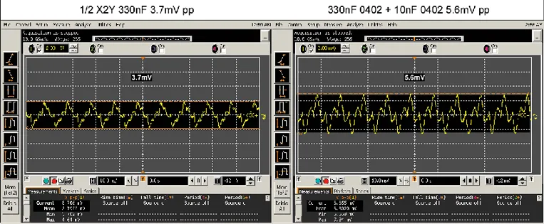
- EMI 3.7mV pp, conventional 5.6mV pp
- Conventional noise 151% greater than EMI
VCC_15V-
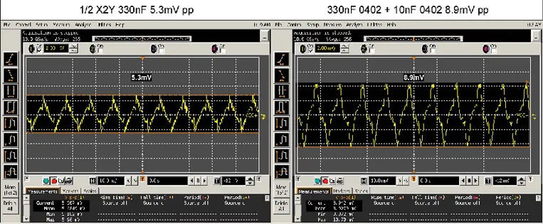
- EMI 5.3mV pp, conventional 8.9mV pp
- Conventional noise 168% greater than EMI
Compare Bypass Conventional MLCC vs. EMI
Test #2
- Amplifier power pin pattern amenable to EMI “circuit 2” use
– the +/- power pins are on the same side of the device - Compares single EMI 100nF rated (200nF total) per pin vs. a single MLCC 220nF per pin

PCB Configuration
Test #2
- Ground attachment is matched between set-ups
- Capacitor set-backs are matched between set-ups
- Compares single EMI 100nF rated (200nF total) per pin vs. a single MLCC 220nF per pin
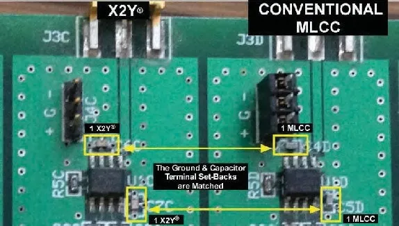
VCC_15V-
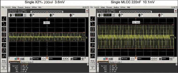
- EMI 3.6mV pp, conventional 10.1mV pp
- Conventional noise 280% greater than EMI
VCC_15V+

- EMI 4.9mV pp, conventional 17.3mV pp
- Conventional noise 353% greater than EMI
Summary
Test #1
- Conventional filter using two capacitor values per power pin, four capacitors total results in >= 150% voltage noise compared to just one EMI used for both power pins.
Test #2
- Conventional filter using one capacitor value per power pin, two capacitors total results in >= 280% voltage noise compared to one EMI used for each power pin.
- Benefits: smaller space, fewer parts, better economy and performance when using EMI components.