Skip navigation

PCB Pad Layout Recommendations

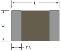
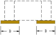
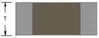
Solder pad design, solder application, and component placement are important elements of the soldering process. Excessive transfer of thermal or mechanical stresses to the MLC can result from oversized solder fillets. Nominal pad designs suitable for the solder reflow process are displayed in the interactive land pattern generator. These guidelines represent a starting point in Printed Circuit Board (PCB) design. For further information on the land pattern design, refer to the standard IPC-SM-782A “Surface Mount Design and Land Pattern Standard” published by the Institute for Interconnecting and Packaging Electronic Circuits (www.ipc.org).

Component Placement Considerations and Pitfalls
Solder pad design, solder application, and accuracy of component placement each must be considered when laying out circuits. This is especially true for RF and microwave circuits where incorrect or asymmetrical deployment of these parameters can lead to serious high frequency performance degradation. Designers beware. IPC-SM-782 is an excellent reference document for optimum soldering of components. However, blindly following this standard can lead to less than optimum high frequency performance and or high voltage issues. If you are not concerned with RF performance or high voltage requirements, Johanson recommends that designers follow this standard (IPC-SM-782). However, for those concerned with RF performance, we recommend a smaller land pattern (solder pad).

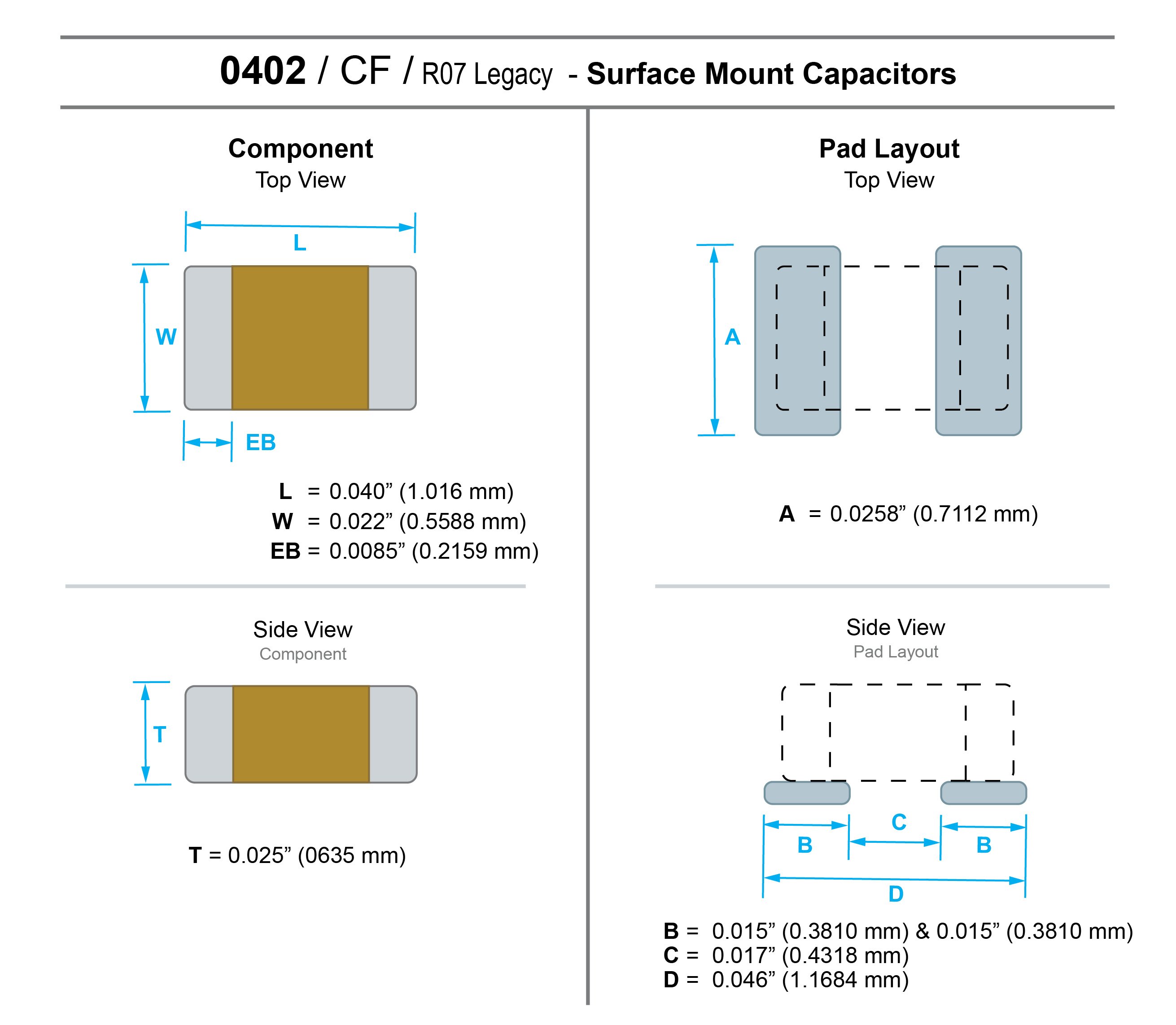
Recommended PCB copper pad layout and footprint dimensions for 0402 (R07) surface mount ceramic capacitor. Diagram shows recommended pad width, length, solder mask clearance and component placement according to Johanson Dielectrics guidelines.
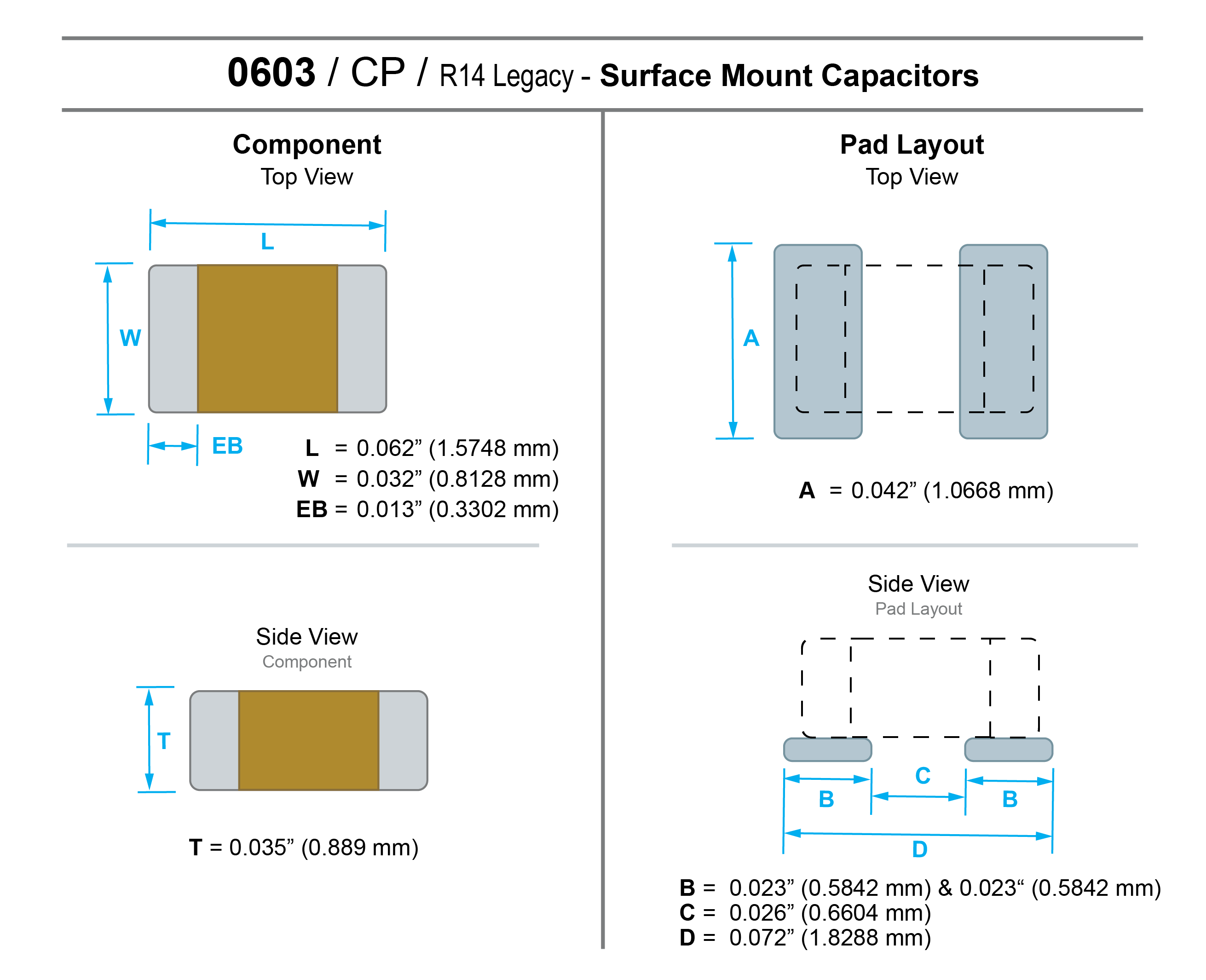
Recommended PCB copper pad layout and footprint dimensions for 0603 (R14) surface mount ceramic capacitor. Diagram shows recommended pad width, length, solder mask clearance and component placement according to Johanson Dielectrics guidelines.
0805 / R15  
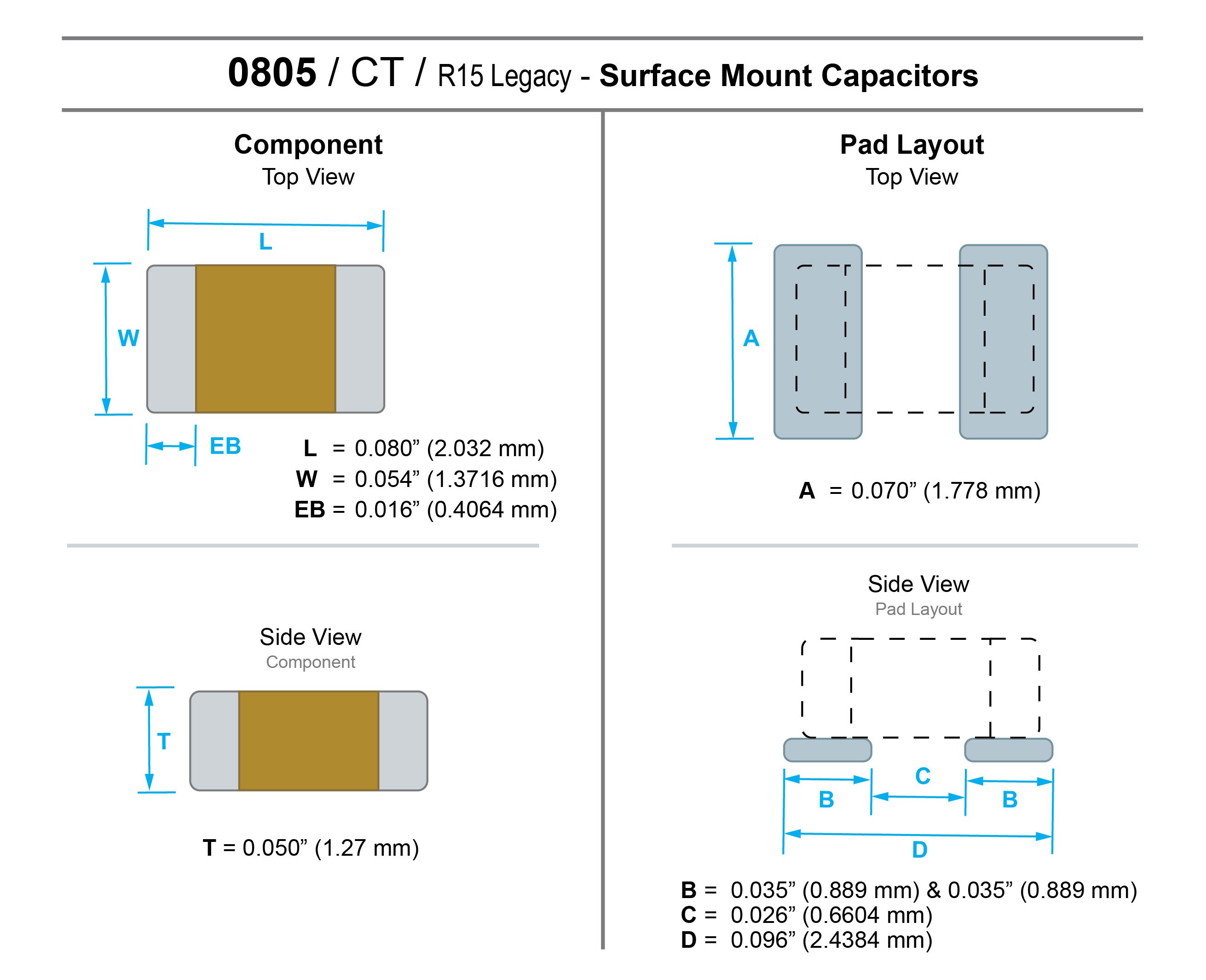
Recommended PCB copper pad layout and footprint dimensions for 0805 (R15) surface mount ceramic capacitor. Diagram shows recommended pad width, length, solder mask clearance and component placement according to Johanson Dielectrics guidelines.
1111 / S42  
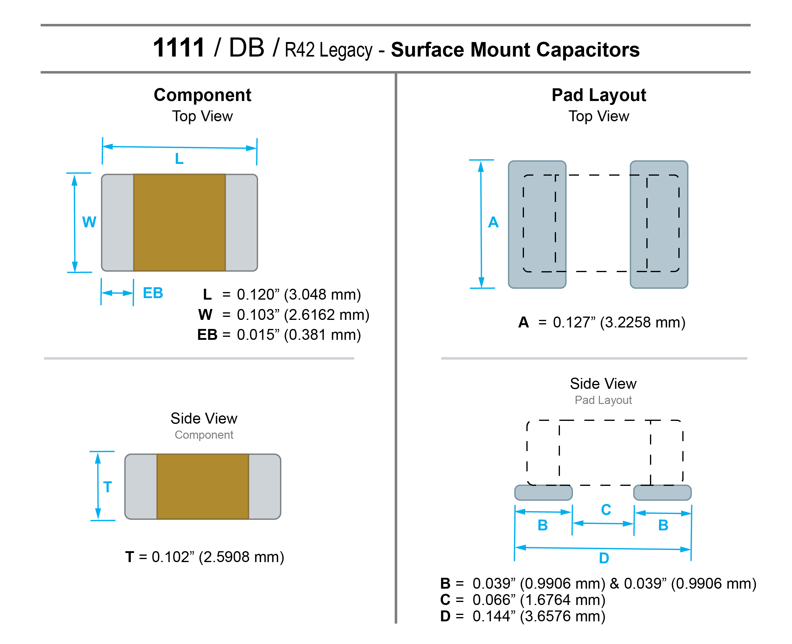
Recommended PCB copper pad layout and footprint dimensions for 1111 (S42) surface mount ceramic capacitor. Diagram shows recommended pad width, length, solder mask clearance and component placement according to Johanson Dielectrics guidelines.
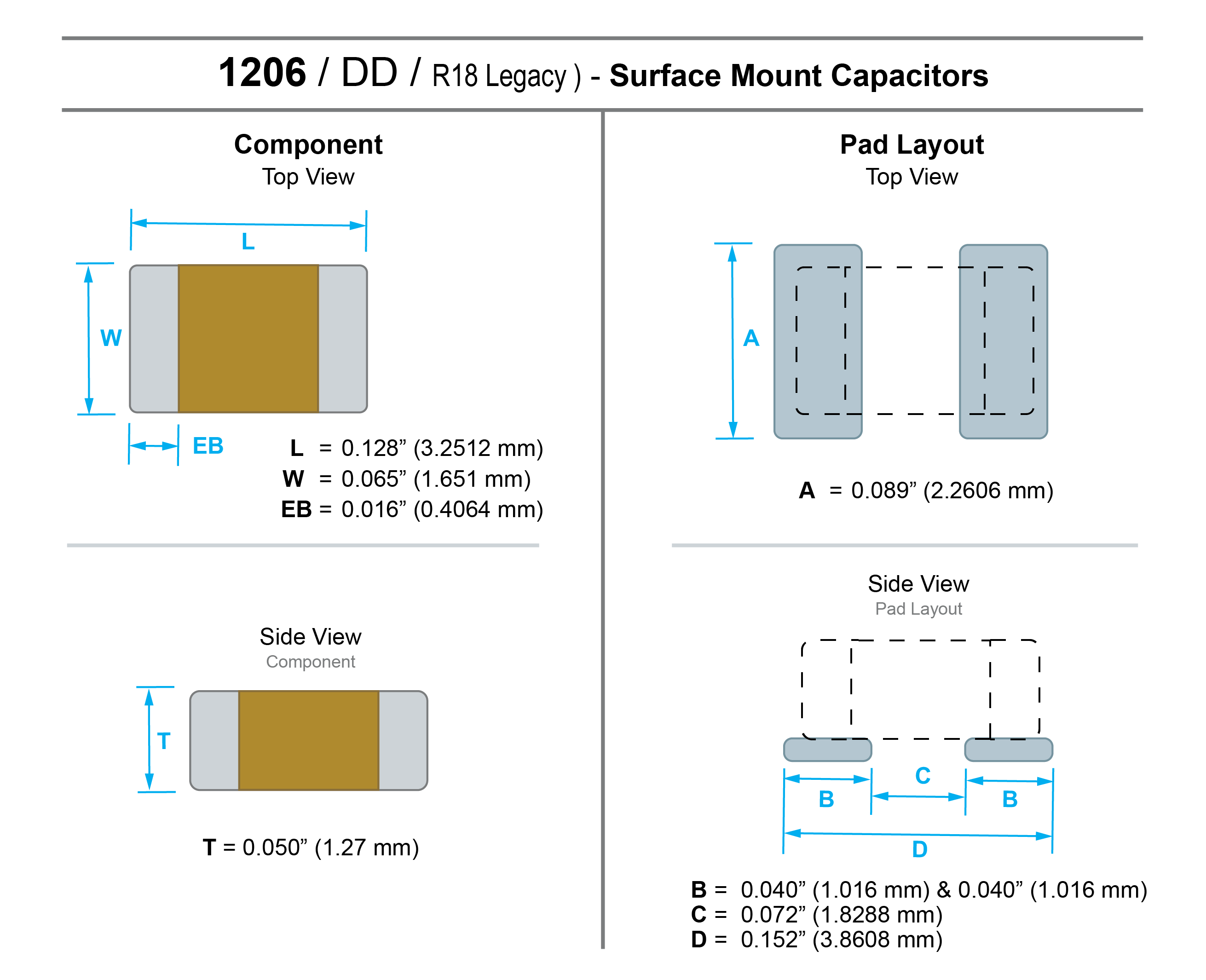
1206 / R18  
Recommended PCB copper pad layout and footprint dimensions for 1206 (R18) surface mount ceramic capacitor. Diagram shows recommended pad width, length, solder mask clearance and component placement according to Johanson Dielectrics guidelines.
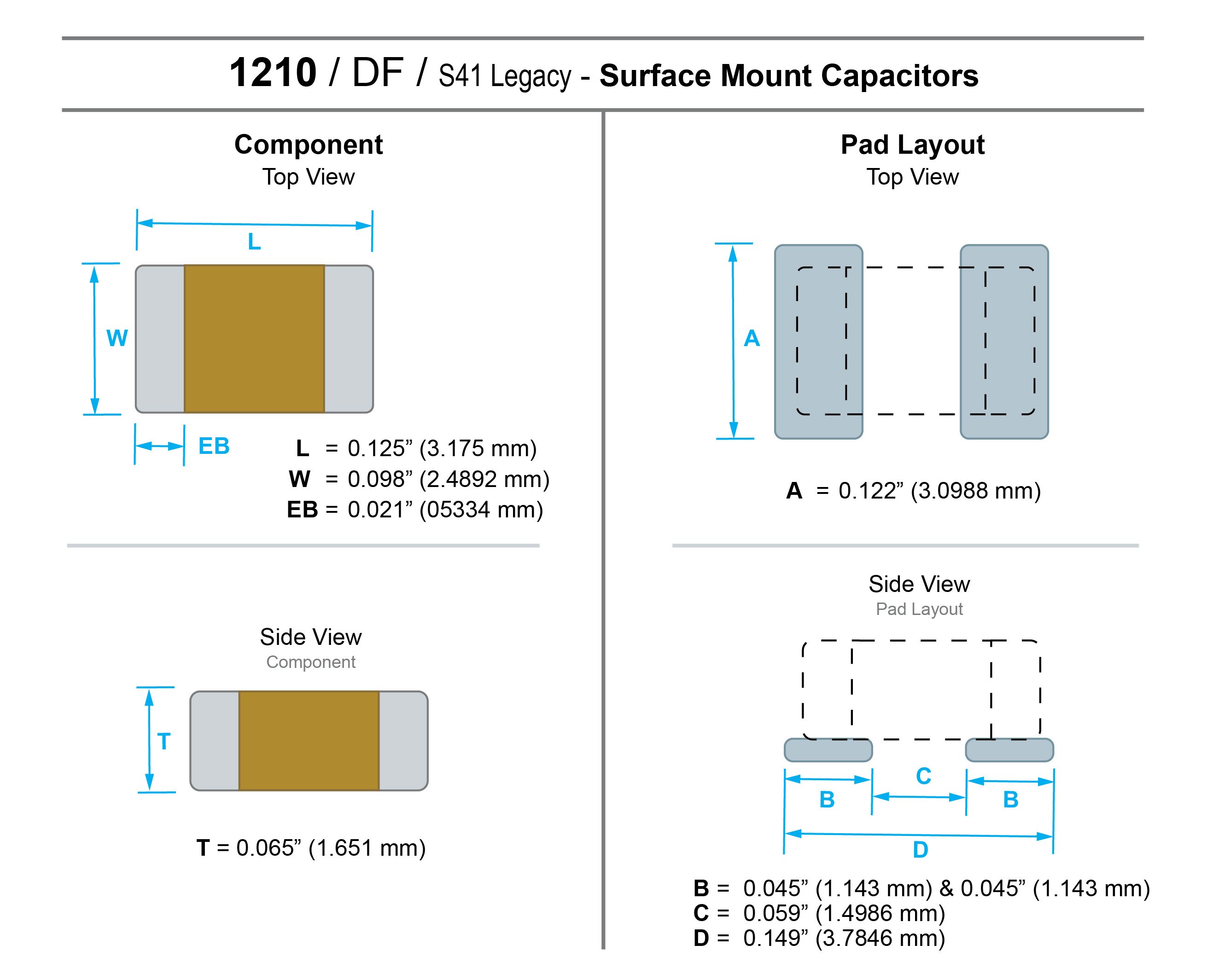
1210 / S41  
Recommended PCB copper pad layout and footprint dimensions for 1210 (S41) surface mount ceramic capacitor. Diagram shows recommended pad width, length, solder mask clearance and component placement according to Johanson Dielectrics guidelines.
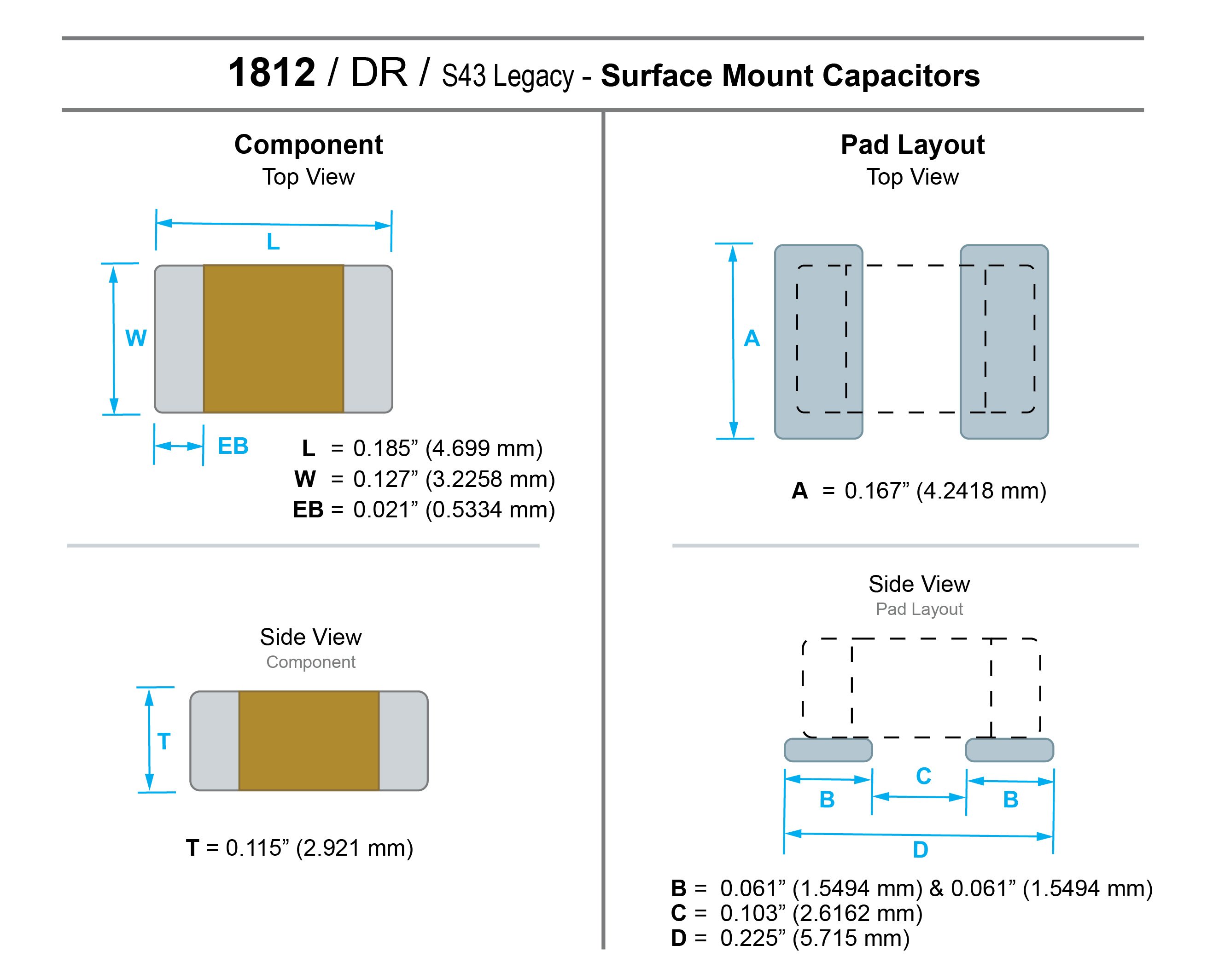
1812 / S43  
Recommended PCB copper pad layout and footprint dimensions for 1812 (S43) surface mount ceramic capacitor. Diagram shows recommended pad width, length, solder mask clearance and component placement according to Johanson Dielectrics guidelines.
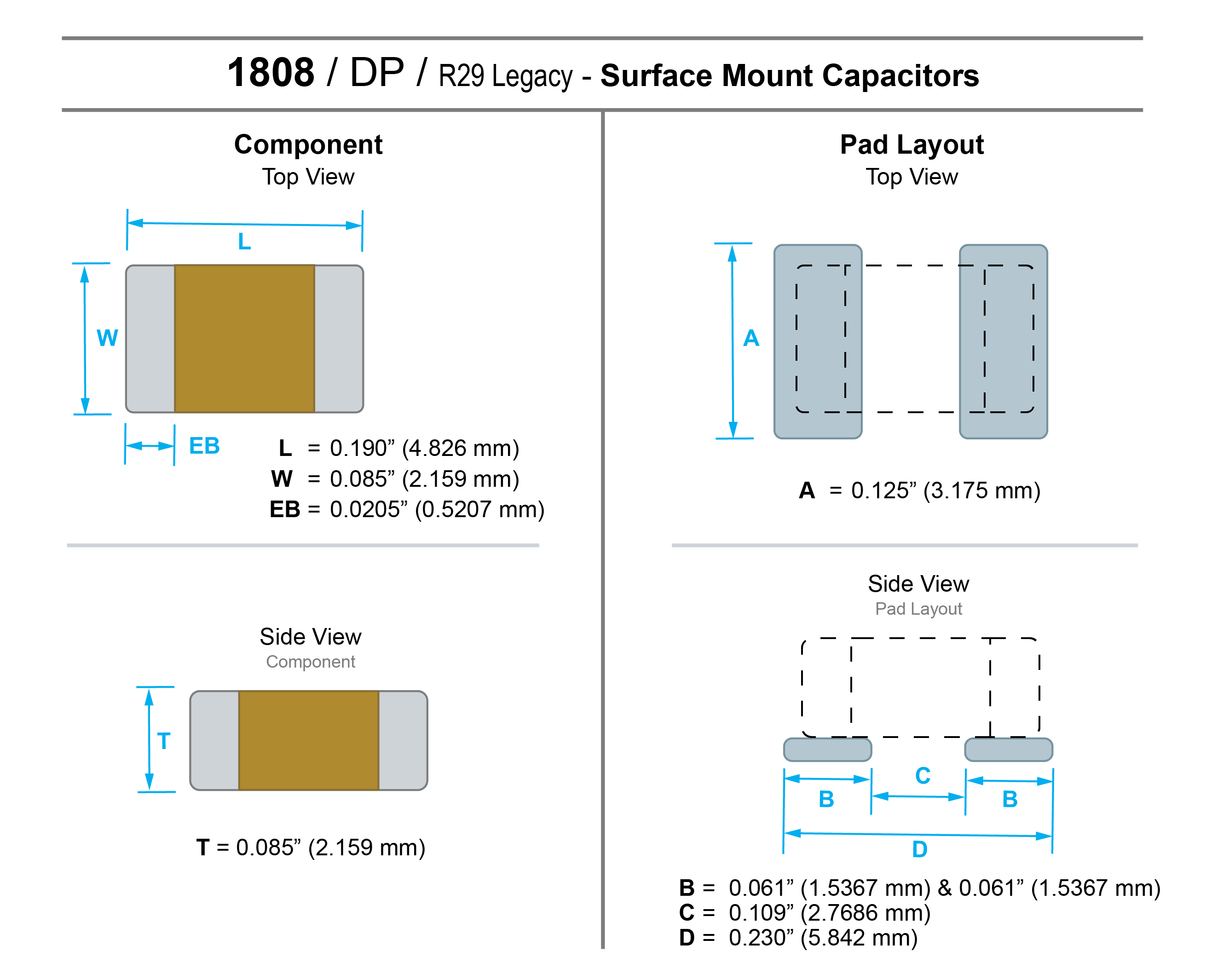
1808 / R29  
Recommended PCB copper pad layout and footprint dimensions for 1808 (R29) surface mount ceramic capacitor. Diagram shows recommended pad width, length, solder mask clearance and component placement according to Johanson Dielectrics guidelines.
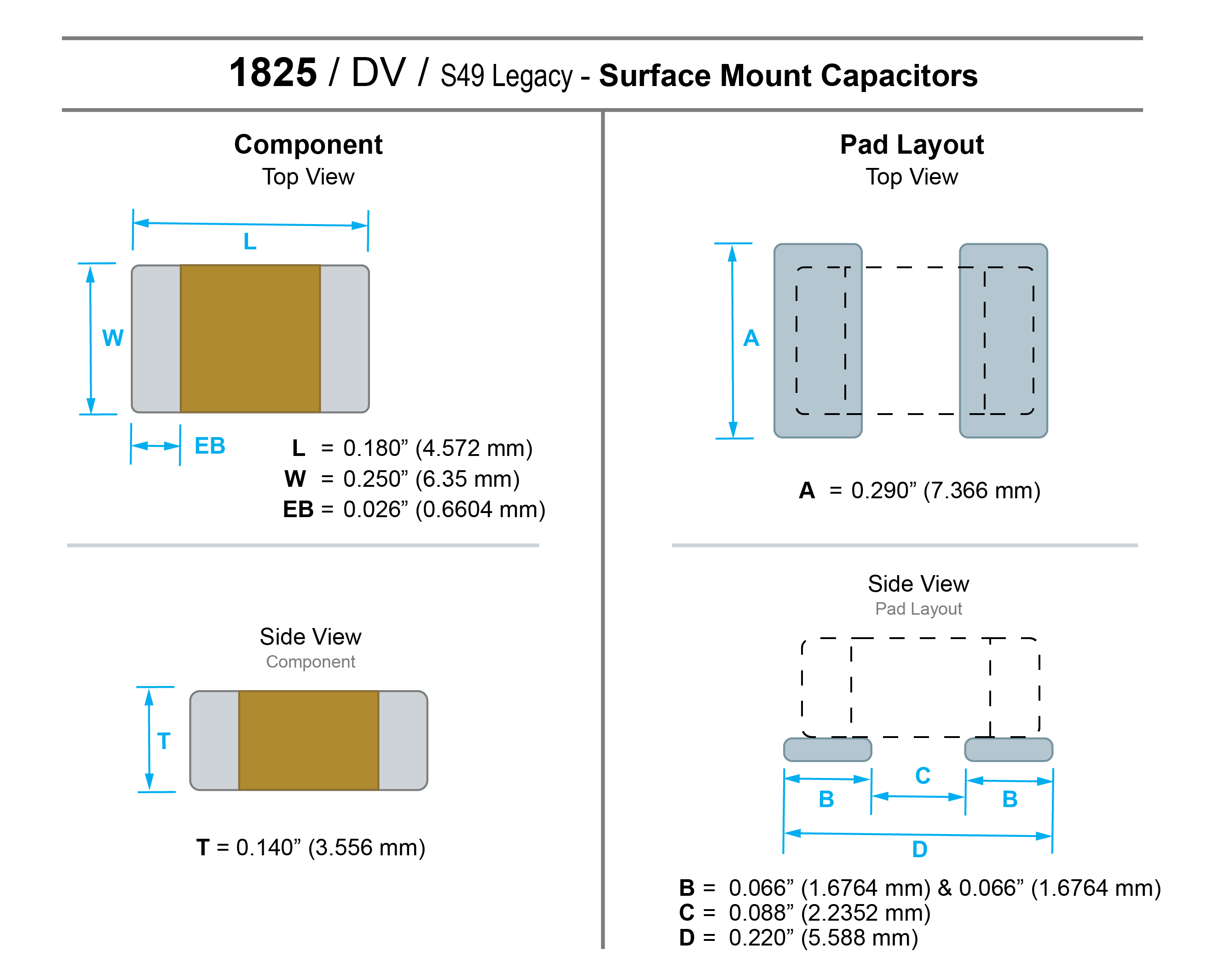
1825 / S49  
Recommended PCB copper pad layout and footprint dimensions for 1825 (S49) surface mount ceramic capacitor. Diagram shows recommended pad width, length, solder mask clearance and component placement according to Johanson Dielectrics guidelines.
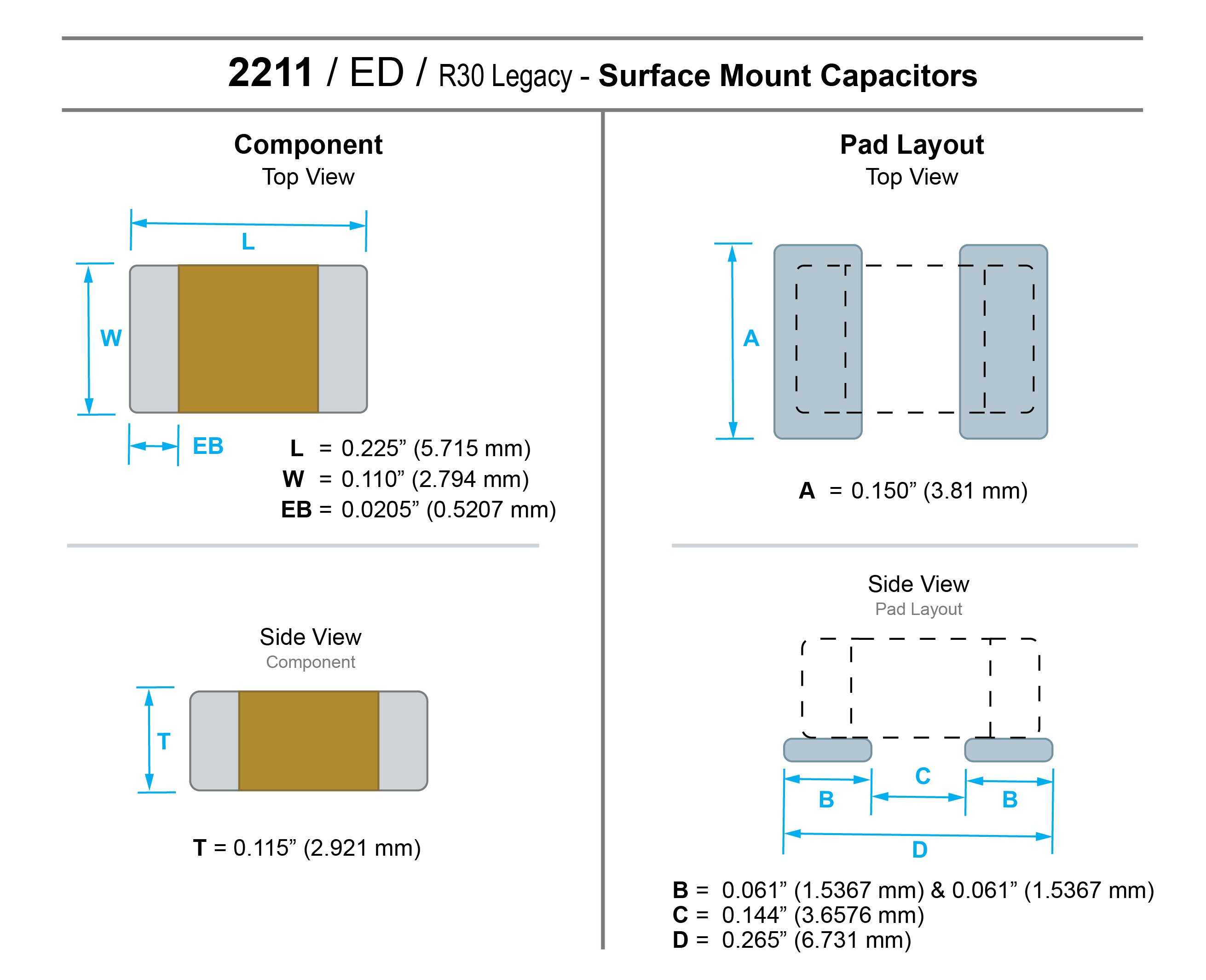
2211 / R30  
Recommended PCB copper pad layout and footprint dimensions for 2211 (R30) surface mount ceramic capacitor. Diagram shows recommended pad width, length, solder mask clearance and component placement according to Johanson Dielectrics guidelines.
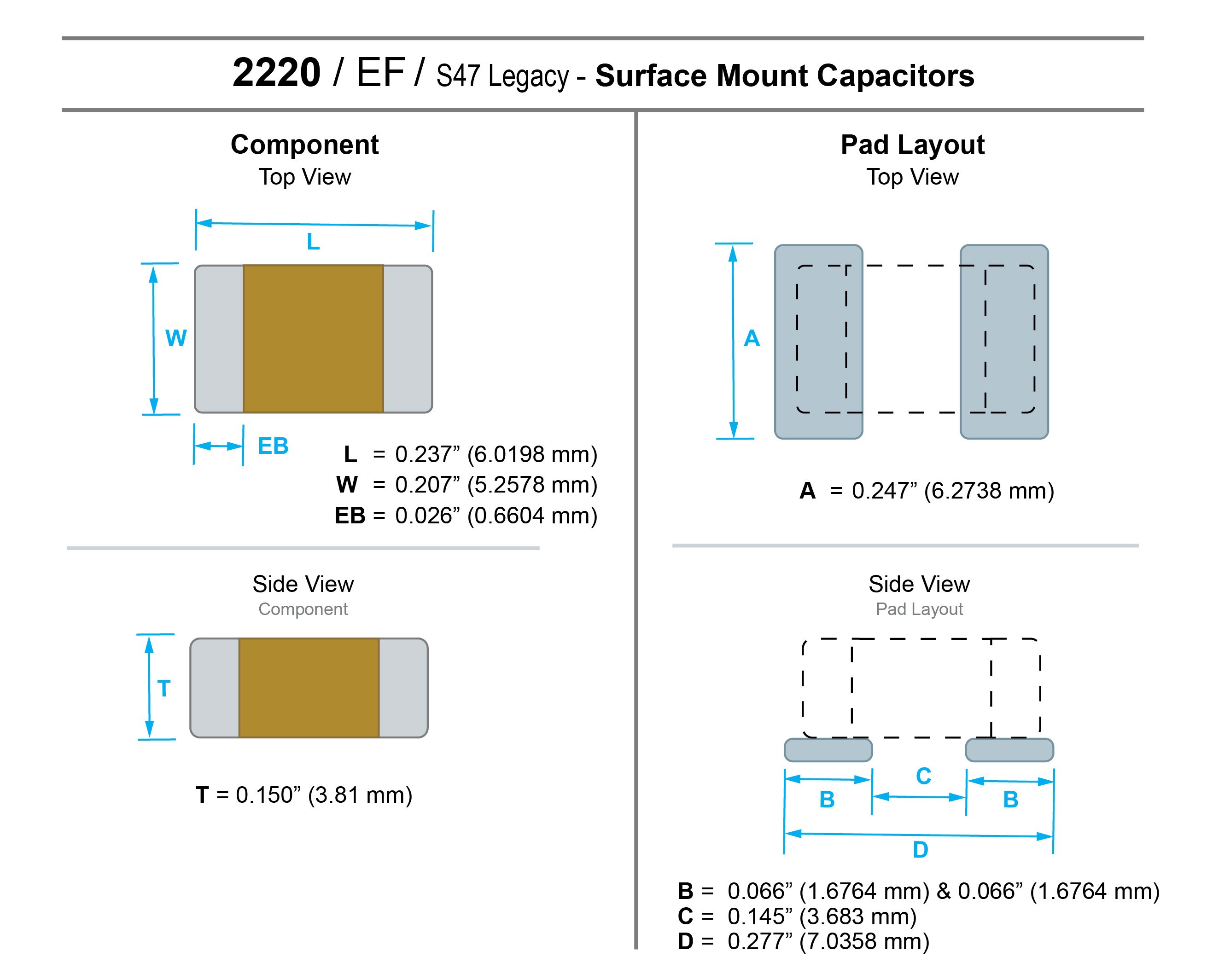
2220 / S47  
Recommended PCB copper pad layout and footprint dimensions for 2220 (S47) surface mount ceramic capacitor. Diagram shows recommended pad width, length, solder mask clearance and component placement according to Johanson Dielectrics guidelines.
2225 / S48  


0.322
(8.1788)

Detail view of recommended PCB pad dimension 0.322 in (8.1788 mm) showing overall length for 2225 (S48) capacitor pad layout


0.262
(6.6548)
0.230 (5.842)
Detail view of recommended PCB pad dimension 0.230 in (5.842 mm) showing pad width for 2225 (S48) capacitor layout
0.026(0.6604)
 
Detail view of recommended PCB pad and solder mask dimensions showing symmetric pad layout for 2225 (S48) capacitor
0.086
(2.1844)
0.086
(2.1844)
Detail view of recommended solder mask opening dimension for 2225 (S48) capacitor pad layout
0.118 (2.9972)
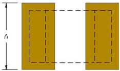
Detail view of recommended PCB pad dimension 0.290 in (7.366 mm) for 2225 (S48) capacitor layout
0.290 (7.366)

0.160
(4.064)
Detail view of recommended PCB pad dimension 0.160 in (4.064 mm) showing pad extension for 2225 (S48) capacitor layout
2525 / S48E  


2.80
(7.112)

Detail view of recommended PCB pad dimension 2.80 in (7.112 mm) showing overall length for 2525 (S48E) capacitor pad layout


0.250
(6.350)
0.230 (5.842)
Detail view of recommended PCB pad dimension 0.230 in (5.842 mm) showing pad width for 2525 (S48E) capacitor layout
0.25(0.635)
 
Detail view of recommended PCB pad and solder mask dimensions showing symmetric pad layout for 2525 (S48E) capacitor
0.050
(1.270)
0.050
(1.270)
Detail view of recommended solder mask opening dimension for 2525 (S48E) capacitor pad layout
0.300 (7.620)
Detail view of recommended PCB pad dimension showing component spacing for 2525 (S48E) capacitor layout
0.400 (10.16)

0.150
(0.381)
Detail view of recommended PCB pad dimension 0.150 in (3.81 mm) showing pad extension for 2525 (S48E) capacitor layout
3838 / S58  


0.434
(11.0236)

Detail view of recommended PCB pad dimension 0.434 in (11.0236 mm) showing overall length for 3838 (S58) capacitor pad layout


0.380
(9.65)
0.380 (9.65)
Detail view of recommended PCB pad dimension 0.380 in (9.65 mm) showing pad width for 3838 (S58) capacitor layout
0.025(0.63)
 
Detail view of recommended PCB pad and solder mask dimensions showing symmetric pad layout for 3838 (S58) capacitor
0.090
(2.286)
0.090
(2.286)
Detail view of recommended solder mask opening dimension for 3838 (S58) capacitor pad layout
0.266 (6.7564)
Detail view of recommended PCB pad dimension showing component spacing for 3838 (S58) capacitor layout
0.446 (11.3284)

0.170
(4.32)
Detail view of recommended PCB pad dimension 0.170 in (4.32 mm) showing pad extension for 3838 (S58) capacitor layout

Performance
For good performance, engineers designing PCBs should consider the following recommendations for Johanson Passives:

  • Pad Size
    • Johanson recommends smaller pad size when compared to the IPC standard. This is done to achieve a compromise between the best RF performance and optimum solderability.
    • Large pad sizes like those recommended by the IPC-SM-782 standard will have RF impedance effects (which can be negative)
  • Pad Symmetry
    • Symmetrical land patterns (pads) are recommended to achieve better RF performance and reduce the likelihood of tombstoning
  • Solder Fillet
    • Solder fillet size can shift impedance at microwave frequencies. Johanson recommends smaller size fillets and consistent size fillets. Large wavelengths tend to be more forgiving with excess solder. Fillets at higher frequencies (very small wavelengths) are much more affected by poor soldering methods. Johanson recommends that the solder fillet be at the lower tolerances in order to minimize RF disruption.
    • Controlling the solder fillet to the low side is an effort to minimize negative impedance effects that occur at higher frequencies.
    • o Smaller solder fillets minimizes thermal and physical stresses

Safety Capacitors
Caution for Safety Caps layouts – Layouts should meet the 3mm (0.1182”) or 4mm (0.1575”) minimum creepage distance between pads as required in the UL or TUV specifications. Here the creepage distance is defined by the “C” dimension in the layout above.