CapStrate® Bulk Capacitance Embedded in a High-k Ceramic Substrate

Embedded Bulk Capacitance for High-Reliability, Space-Saving PCB Designs
Overiew:
CapStrate® is an integrated multilayer ceramic capacitor structure designed to reduce parasitic inductance in high-speed discharge applications. By incorporating the switch and associated trigger circuitry directly onto the CapStrate® surface, overall circuit length is minimized. This reduction in loop length lowers parasitic inductance, resulting in improved pulse shape control and more consistent energy delivery.
Key Features:
- Customizable to accommodate challenging board layouts "Space Saver"
- Quick turn prototype to high volume production
- Reducing component count and higher reliability
- Unique customer solutions
- One-stop design, manufacturing, and assembly
Choosing the correct CapStrate® influences the mechanical and electrical function of a design. Johanson Dielectrics offers ceramic substrates for use in application specific environments. It is recommended to choose the right substrate that meets the required electrical requirements and is suitable for the environment the product will operate in.
Johanson Dielectrics offers a variety of materials with a high dielectric constant (K) that can be used within CapStrate® designs. The dielectric constant is directly related to the amount of bulk capacitance that can be realized and allows for compact form factors.
Table 1: Available CapStrate® & Electrical Properties
| CapStrate® Material | X7R | NP0 | X8R |
|---|---|---|---|
| Dissipation Factor | <2.5% | <0.15% | <2.5% |
| Dielectric Strength (V/mil) | 200 | 300 | 200 |
| Temperature Coefficient | ±15% | 0 ± 30 ppm/°C | ±15% |
| Temperature Range | -55 °C to +125 °C | -55 °C to +125 °C | -55 °C to +150 °C |
CapStrate® Sizes & Shapes
Table 2: Rectangular Dimensions (CapStrate®)
| Dimension | Minimum | Maximum | Tolerance |
|---|---|---|---|
| Thickness | 0.050” (1.27mm) | 0.215” (5.461mm) | +/- 0.005 (0.127mm) |
| Length | 0.20” (5.08mm) | 2.00”/1.00” (50.8/25.4mm) | +/- 0.005 (0.127mm) |
| Width | 0.20” (5.08mm) | 1.00”/2.00” (25.4/50.8mm) | +/- 0.005 (0.127mm) |
| Temperature Range | -55 °C to +125 °C | -55 °C to +125 °C | -55 °C to +150 °C |
Table 3: Circular Dimensions (CapStrate®)
| Dimension | Minimum | Maximum | Tolerance |
|---|---|---|---|
| Thickness | 0.050” (1.27mm) | 0.215” (5.46mm) | +/- 0.005 (0.127mm) |
| Diameter | 0.20” (5.08mm) | 2.00” (50.8mm) | +/- 0.005 (0.127mm) |
The advantages of CapStrate® Dielectrics can be fully realized by replacing discrete capacitors with bulk capacitance from the ceramic substrates. The amount of capacitance that can be utilized varies depending on the design dimensions.
Tables 4 and 5 reference the maximum amount of capacitance that can be designed for dimensional, substrate and voltage constraints.
Typical voltage ratings vary from 100 to 1000V, however, engineers are invited to discuss special voltage requirements not listed below.

Table 4: Rectangular Bulk Capacitance (CapStrate®)
| NP0 | Length | Width | Thickness | 100V | 250V | 500V | 1000V |
|---|---|---|---|---|---|---|---|
| Maximum Size | 2.00” (50.8mm) | 1.00” (25.4mm) | 0.150” (3.81mm) | 5000nF | 2500nF | 1400nF | 940nF |
| Minimum Size | 0.20” (5.08mm) | 0.20” (5.08mm) | 0.050” (1.27mm) | 30nF | 9nF | 5nF | 2.8nF |
| X7R | Length | Width | Thickness | 100V | 250V | 500V | 1000V |
|---|---|---|---|---|---|---|---|
| Maximum Size | 2.00” (50.8mm) | 1.00” (25.4mm) | 0.150” (3.81mm) | 120000nF | 60000nF | 25000nF | 8000nF |
| Minimum Size | 0.20” (5.08mm) | 0.20” (5.08mm) | 0.050” (1.27mm) | 800nF | 200nF | 70nF | 20nF |
| X8R | Length | Width | Thickness | 100V | 250V | 500V | 1000V |
|---|---|---|---|---|---|---|---|
| Maximum Size | 2.00” (50.8mm) | 1.00” (25.4mm) | 0.150” (3.81mm) | 84000nF | 42000nF | 17500nF | 5600nF |
| Minimum Size | 0.20” (5.08mm) | 0.20” (5.08mm) | 0.050” (1.27mm) | 560nF | 140nF | 49nF | 14nF |
- Custom Geometry
- Increased Bulk Capacitance
- High Voltage Capabilities
- Reduction in Size
Table 5: Circular Bulk Capacitance (CapStrate®)
| NP0 | Diameter | Thickness | 100V | 250V | 500V | 1000V | 10000V |
|---|---|---|---|---|---|---|---|
| Maximum Size | 2.00” (50.8mm) | 0.150” (3.81mm) | 7600nF | 3800nF | 2600nF | 1400nF | 940nF |
| Minimum Size | 0.20” (5.08mm) | 0.050” (1.27mm) | 25nF | 6nF | 3nF | 1.7nF | 2.8nF |
| X7R | Diameter | Thickness | 100V | 250V | 500V | 1000V | 10000V |
|---|---|---|---|---|---|---|---|
| Maximum Size | 2.00” (50.8mm) | 0.150” (3.81mm) | 180000nF | 95000nF | 40000nF | 12000nF | 8000nF |
| Minimum Size | 0.20” (5.08mm) | 0.050” (1.27mm) | 550nF | 140nF | 45nF | 15nF | 20nF |
| X8R | Diameter | Thickness | 100V | 250V | 500V | 1000V | 10000V |
|---|---|---|---|---|---|---|---|
| Maximum Size | 2.00” (50.8mm) | 0.150” (3.81mm) | 126000nF | 66500nF | 28000nF | 8400nF | 5600nF |
| Minimum Size | 0.20” (5.08mm) | 0.050” (1.27mm) | 385nF | 98nF | 31.5nF | 10.5nF | 14nF |
Additional sizes and form factors not listed are possible. Contact Johanson to assess the feasibility of your design. Reference table 6 for the maximum capacitance density that can be used for a given substrate. Capacitance density, below, is presented in nF/(mils)3. This is the maximum amount of capacitance available in a given volume.
Table 6: Max Capacitance Density
| Rectangular | X7R | NP0 | X8R | Circular | X7R | NP0 | X8R |
|---|---|---|---|---|---|---|---|
| 100V | 4.00E-04 | 1.67E-05 | 2.80E-04 | 100V | 3.82E-04 | 1.61E-02 | 1.13E-02 |
| 250V | 2.00E-04 | 8.33E-06 | 1.40E-04 | 250V | 2.02E-04 | 8.10E-03 | 5.67E-03 |
| 500V | 8.33E-05 | 4.67E-06 | 5.83E-05 | 500V | 8.49E-05 | 5.51E-03 | 3.86E-03 |
| 1000V | 2.67E-05 | 3.13E-06 | 1.87E-05 | 1000V | 2.54E-05 | 2.97E-03 | 2.08E-03 |
Johanson Dielectrics offers a variety of metallization schemes that are high reliability conductors. These metals can be utilized as conductors, solder pads, or methods of thermal transfer. Designers should select the available metal based on the metallization properties that best suit their design. Careful selection of particular metallizations is dependent on requirements for solderability, temperature resistance, and electrical performance.
Table 7: Metallization Schemes Available
| Dielectric | Ag / Pt | Ni / Au | Ag / Ni / Au |
|---|---|---|---|
| X7R | X | X | - |
| X8R | X | X | - |
| NP0 | X | - | X |
Table 8: Metallization Properties
| Material Property | Ag / Pt | Ni / Au | Ag / Ni / Au |
|---|---|---|---|
| Recommended Thickness | 14µm | 7-12µ” | Contact Factory |
| Max Solder Temp | 218°C | 260°C | 230°C |
Table 9: Solder Pad Dimensions
| Metallization | Length (Minimum) | Width (Minimum) | Pad Spacing (Minimum) |
|---|---|---|---|
| Ag/Pt | 0.015" (0.381mm) | 0.010" (0.254mm) | 0.007" (0.178mm) |
| Ni/Au | 0.015" (0.381mm) | 0.010" (0.254mm) | 0.007" (0.178mm) |
| Ag/Ni/Au | 0.015" (0.381mm) | 0.010" (0.254mm) | 0.007" (0.178mm) |
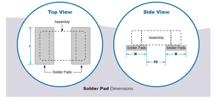
Table 10: Standard Conductor Traces & Tolerances
| Metallization | Line Width / Space (Min) | Line Width / Space Tolerance (Max) | Trace / Metal Thickness |
|---|---|---|---|
| Ag/Pt | 0.007” (0.178mm) | 0.003”-0.005” (0.076-0.127mm) | 0.014” (0.356mm) |
| Ni/Au | 0.007” (0.178mm) | 0.003”-0.005” (0.076-0.127mm) | 0.014” (0.356mm) |
| Ag/Ni/Au | Ag/Ni/Au | 0.003”-0.005” (0.076-0.127mm) | 0.014” (0.356mm) |

Vias are used to connect different layers in the CapStrate® as a means of an electrical or thermal connection. Johanson Dielectrics offers plated through-hole vias for designers to use
Table 11: Via Mechanical Dimensions
| Via Style | Hole Diameter (Minimum) | Hole to Hole (Minimum Spacing) | Via to Edge (Minimum Spacing) |
|---|---|---|---|
| Plated Through-hole | 0.028” (0.771mm) | 0.012” (0.305mm) | 0.015” (0.381mm) |

We encourage all designers to submit their drawings or ideas for quick and easy feedback.
To submit:
- Follow Johanson’s design guidelines and standard specifications
- Provide CAD data in multiple layers
- Identify “A” side and “B” side for double-patterned circuits
- Provide tolerances and annotation
- List CapStrate® type, dimensions, and rated voltage
- Specify metallizations, thickness and tolerances, pads
- Specify conductor traces, type, spacing, and tolerances
- List any environmental or electrical testing needed
- Other inspection or acceptance criteria
Don't miss the opportunity to work with our outstanding design engineers.
Send us a message for more information. We look forward to assisting you with your unique design requirements.
Assembly Services
Available in-house
Includes but is not limited to, soldering resistors, inductors, wires and transistors.
One-stop design, manufacturing, and assembly ensures customers receive completed product, without the hassle of developing an assembly stations.
What is CapStrate®?
CapStrate® from Johanson Dielectrics is an integrated multilayer ceramic capacitor structure that embeds bulk capacitance into a high-k ceramic substrate. It is designed to reduce parasitic inductance in high-speed discharge applications while supporting compact, application-specific designs.
How can I reduce parasitic inductance in a high-speed discharge circuit?
CapStrate® allows the switch and associated trigger circuitry to be incorporated directly onto the capacitor substrate. This minimizes overall circuit and loop length, reducing parasitic inductance and improving pulse shape control and energy delivery consistency.
How does CapStrate® improve pulse discharge performance?
CapStrate® reduces circuit loop length by placing switching and trigger circuitry directly on the capacitor surface. The resulting reduction in parasitic inductance provides improved pulse shape control and more consistent energy delivery.
Can capacitance be embedded directly into a ceramic substrate?
Yes. CapStrate® integrates bulk capacitance directly into a high-k ceramic substrate, allowing designers to replace discrete capacitors with capacitance contained within the ceramic substrate itself.
How can I reduce capacitor component count in a circuit?
CapStrate® enables discrete capacitors to be replaced with bulk capacitance integrated into the ceramic substrate. Johanson identifies reduced component count and higher reliability among the key features of the technology.
What is the advantage of a high-k ceramic substrate?
Johanson Dielectrics offers high dielectric constant (high-k) materials for CapStrate® designs. The dielectric constant is directly related to the amount of bulk capacitance that can be achieved, helping enable compact form factors.
Is CapStrate® suitable for space-constrained circuit designs?
Yes. CapStrate® can be customized to accommodate challenging board layouts and is specifically identified by Johanson as a“Space Saver.” High-k materials also enable bulk capacitance in compact form factors.
What voltage ratings are available for CapStrate®?
Typical CapStrate® voltage ratings range from 100 to 1000 V. Johanson Dielectrics also invites engineers to discuss special voltage requirements outside the listed range.
How much capacitance can be embedded in a CapStrate®?
The amount of bulk capacitance available depends on the design dimensions, substrate, and voltage constraints. Johanson provides capacitance-density information to help determine the maximum capacitance available within a given volume.
Can CapStrate® be customized for my circuit layout?
Yes. Johanson Dielectrics offers custom CapStrate® solutions, including additional sizes and form factors beyond those listed in its standard design information. Designers can submit drawings or design concepts for feasibility review.
Can components be mounted directly onto CapStrate®?
Yes. Johanson states that components including resistors, inductors, wires, and transistors can be incorporated as part of its assembly offering.
Does CapStrate® support plated through-hole vias?
Yes. Johanson Dielectrics offers plated through-hole vias for CapStrate®. Vias can connect different layers and provide electrical or thermal connections within the structure.
What metallization options are available for CapStrate®?
Johanson Dielectrics offers multiple high-reliability metallization schemes that can function as conductors, solder pads, or methods of thermal transfer. Metallization selection depends on requirements including solderability, temperature resistance, and electrical performance.
Can Johanson manufacture and assemble a custom CapStrate® design?
Yes. Johanson offers design, manufacturing, and assembly for CapStrate® solutions, from quick-turn prototypes through high-volume production.
What information is needed for a custom CapStrate® design?
Johanson recommends providing the CapStrate® type, dimensions, rated voltage, metallization requirements, thicknesses and tolerances, pads, conductor traces and spacing, and any required environmental or electrical testing. For double-patterned circuits, designers should also identify the A and B sides.