Understanding Ceramic Capacitor Terminations
John Maxwell, Director of Product Development
The relationship between termination and ceramic body is critical in understanding stress concentration, crack formation due to heat, mechanical flexure and solder joint stress and resulting leakage current conduction. Capacitor hermetic performance is also dictated by the relationship between termination and ceramic body.
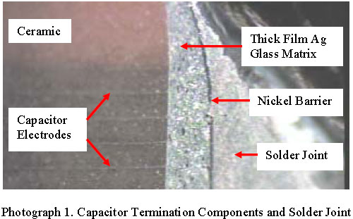
A ceramic capacitor termination is not solid metal but a composite of structures built upon one another. During manufacturing after a capacitor is fired or sintered each end is dipped in metal glass frit thick film ink consisting of metal particles or flakes and doped borosilicate glass. That ink is then dried and when both ends are coated it is fired or sintered to the ceramic body. During this secondary sintering process the glass particles fuse along contacts with one another creating a matrix or sponge like structure. The glass also diffuses into the ceramic capacitor body to insure adhesion creating a thin zone that has undergone a phase change. The ceramic capacitor body is polycrystalline with the exception of NP0 dielectrics so glass diffusion creates an amphorus boundary layer with different material properties other than either the glass or ceramic. Depending on a number of capacitor manufacturing process parameters this boundary layer may be thick or thin, cracked or not. Thick layers tend to crack during capacitor manufacturing increasing cracking in PWB assembly operations or during normal product use. After the termination has been fired or sintered it is then electroplated with a nickel layer to minimize dissolution during soldering and is finally plated with a solder or tin layer to preserve solderability of the nickel layer. Photograph 1 show ceramic, termination thick film metal, nickel-plated layers and solder.
The function of the glass is to also hold termination precious metal (Ag or PdAg) particles in contact with capacitor electrodes that slightly protrude from the ceramic body. In the case of base metal terminations either copper or nickel metal glass thick film ink is used in conjunction with nickel electrodes.
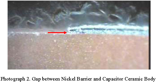
The termination structure is slightly porous allowing air and moisture in the form of humidity to penetrate through that layer. Nickel plating operations and chemistry do not typically allow nickel to be plated directly on the ceramic capacitor surface leaving a small gap between the nickel layer and ceramic body and is shown in Photograph 2.
This is the path for moisture to enter the porous termination structure as the ceramic capacitor body is not porous. This path extends into the ceramic capacitor along electrode surfaces trough the gap between electrode and ceramic. If there is a microscopic crack between opposing electrodes then moisture can completely penetrate the structure and provide the necessary initial conductive path. Water hydrolyzes at .86V breaking down into H+ and OH- ions that conduct current. The free hydrogen atom can easily rob an oxygen atom out of the ceramic along a small crack of flaw surface leaving behind a permanent titanium rich surface. This is critical in understanding long term ceramic capacitor failures in that a part may seem fine during burn in and test but then fail later in the field. More frustrating is when a part is sent out for analysis in that a no problem found is reported. Some times a part can be "Fixed" by touching it with a soldering iron. Once there is a small crack it is not fixed with a soldering iron but over time leakage current increases to the point of permanent capacitor failure.