Untitled Document
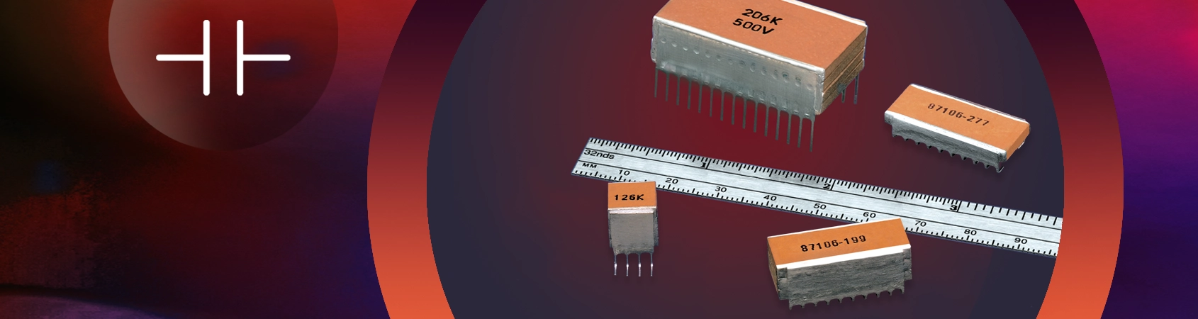
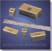
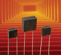
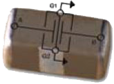
SMPS Switch-Mode Stacked ceramic capacitors feature large capacitance values and exhibit low ESR (equivalent series resistance) and low ESL (equivalent series inductance) making them well suited for high power and high frequency applications where tantalum or aluminum electrolytic capacitors may not be suitable. Johanson offers three series Stacked assemblies. The P-Series feature mechanical and pin-out configurations per DSCC 87106 and 88011 drawings while the E-Series feature mechanical and pin-out configurations more common in European design applications. The T-Series feature 200°C applications.
SMPS Switch-Mode Ceramic Capacitors

Features:

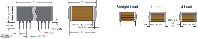
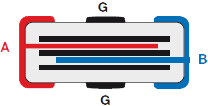
  • E-Series Common European Lead Styles
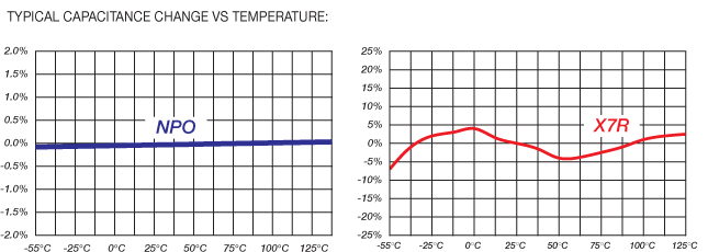
  • NPO & X7R Dielectrics, 50 to 500 VDC Ratings


  • Low ESR / Low ESL, Ideal for SMPS Filtering Applications
  • Custom Sizes, Voltages, and Values Available

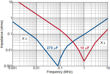
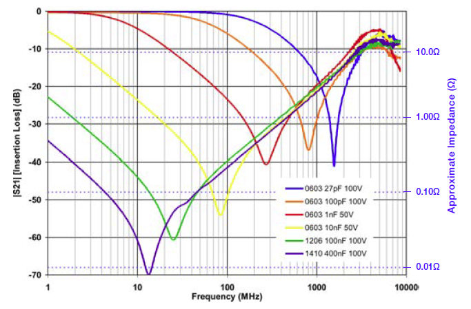
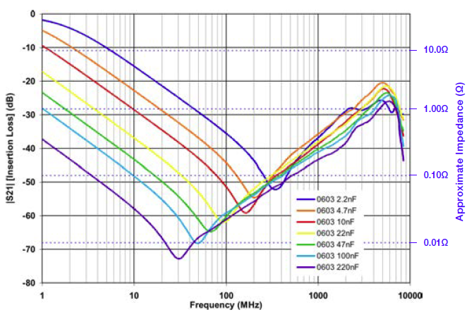
Impedance vs Frequency:

The left-hand portion of the curves represents the capacitive reactance of two typical values. The impedance decreases until series resonance is reached. At this point (the bottom of the V), the only component of the impedance is the ESR. At higher frequencies (the inductive portion) the ESR remains relatively low so that effective filtering is maintained.
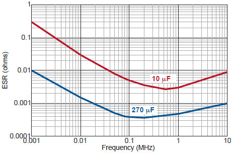
Switchmode Impedance vs Frequency chart

ESR vs Frequency:

These curves reflect the very low ESR of two typical values. These ESRs are much lower than Tantalums or Aluminum electrolytics of the same values. The result is the ability to provide filtering (low loss) and to handle high power requirements.

Switchmode ESR vs Frequency chart

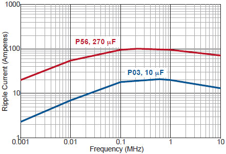
Ripple Current vs Frequency:

Here are two examples of the ability of Switch-Mode capacitors to handle high values of ripple current (high power) at various frequencies. Refer to the "AC Power Computations" applications note or contact Johanson Dielectrics Applications Engineering for more information.

Switchmode Ripple Current vs Frequency chart
Soldering Precautionstary Specifications:

The large ceramic mass of Switch-Mode capacitors increases their susceptibility to damage from thermal shock during soldering. Parts should be pre-heated to within 50°C of the peak soldering temperature and the preheating cycle's thermal gradient should be limited to a maximum of 2°C per second.

P-Series Capacitance Values

P-Series Mechanical Characteristics
Case SizeNP0 Max Capacitance (μF)BX Max Capacitance (μF)X7R Max Capacitance (μF)
50V 100V 200V 500V 50V 100V 200V 500V 50V 100V 200V 500V
P05 0.07 0.05 0.04 0.02 1.3 0.70 0.37 0.17 3.0 2.2 1.0 .50
P25 0.14 0.10 0.08 0.04 2.6 1.4 0.74 0.34 6.0 4.4 2.0 1.0
P35 0.21 0.15 0.12 0.06 3.9 2.1 1.1 0.51 9 6.6 3.0 1.5
P45 0.28 0.20 0.16 0.08 5.2 2.8 1.5 0.68 12 8.8 4.0 2.0
P55 0.35 0.25 0.20 0.10 6.5 3.5 1.8 0.85 15 11 5.0 2.5
P04 0.22 0.15 0.12 0.07 4.0 2.0 1.1 0.50 9 6.5 3.0 1.5
P24 0.44 0.30 0.24 0.14 8.0 4.0 2.2 1.0 18 13 6 3.0
P34 0.66 0.45 0.36 0.21 12 6.0 3.3 1.5 27 19 9 4.5
P44 0.88 0.60 0.48 0.28 16 8 4.4 2.0 36 26 12 6.0
P54 1.1 0.75 0.60 0.35 20 10 5.5 2.5 45 32 15 7.5
P03 0.70 0.50 0.39 0.22 10 6.8 3.5 1.5 28 20 9.5 4.7
P23 1.4 1.0 0.78 0.44 20 13 7.0 3.0 56 40 19 9.4
P33 2.1 1.5 1.2 0.66 30 20 10 4.5 84 60 28 14
P43 2.8 2.0 1.5 0.88 40 27 14 6.0 112 80 38 18
P53 3.5 2.5 2.0 1.1 50 34 17 7.5 140 100 47 23
P01 1.4 1.0 0.75 0.44 20 13 7 3.0 50 40 19 9.4
P21 2.8 2.0 1.5 0.88 40 27 14 6.0 100 80 38 18
P31 4.2 3.0 2.2 1.3 60 40 21 9.0 150 120 57 27
P41 5.6 4.0 3.0 1.8 80 54 28 12 200 160 76 36
P51 7.0 5.0 3.7 2.2 100 68 35 15 250 200 95 46
P02 2.0 1.4 1.0 0.6 30 19 10 5 75 55 25 14
P22 4.0 2.8 2.0 1.2 60 38 20 9 150 110 50 28
P32 6.0 4.2 3.0 1.8 90 57 30 13 220 160 75 42
P42 8.0 5.6 4.0 2.4 120 76 40 18 300 220 100 56
P52 10 7.0 5.0 3.0 150 95 50 22 370 270 125 70
P06 4.0 2.8 2.2 1.2 69 40 20 9 160 110 50 25
P26 8 5.6 4.4 2.4 130 80 40 18 320 220 100 50
P36 12 8.4 6.6 3.6 200 120 60 27 480 330 150 75
P46 16 11 8.8 4.8 270 160 80 36 640 440 200 100
P56 20 14 11 6 340 200 100 45 800 550 250 125

E-Series Capacitance Values

E-Series Capacitance & Voltage Selection
Case SizeNP0 Max Capacitance (μF)BX Max Capacitance (μF)X7R Max Capacitance (μF)
50V 100V 200V 500V 50V 100V 200V 500V 50V 100V 200V 500V
E24 0.13 0.09 0.07 0.045 2.2 1.5 0.8 0.35 5.0 4.0 2.5 1.0
E34 0.26 0.18 0.14 0.09 4.4 3.0 1.6 0.70 10 8.0 5.0 2.0
E44 0.39 0.27 0.21 0.13 6.6 4.5 2.4 1.0 15 12 7.5 3.0
E54 0.52 0.36 0.28 0.18 8.8 6.0 3.2 1.4 20 16 10 4.0
E25 0.22 0.15 0.12 0.08 3.9 2.5 1.4 0.60 9.0 6.5 4.0 1.8
E35 0.44 0.30 0.24 0.16 7.8 5.0 2.8 1.2 18 13 8.0 3.6
E45 0.66 0.45 0.36 0.24 11 7.5 4.2 1.8 27 19 12 5.4
E55 0.88 0.60 0.48 0.32 15 10 5.6 3.0 36 26 16 7.2
E26 0.4 0.30 0.22 0.15 7.0 4.5 2.5 1.0 16 12 7.5 3.3
E36 0.8 0.60 0.44 0.30 14 9.0 5.0 2.0 32 24 15 6.6
E46 1.2 0.90 0.66 0.45 21 13 7.5 3.0 48 36 22 9.9
E56 1.6 1.2 0.9 0.60 28 18 10 4.0 64 48 30 13
E27 0.7 0.5 0.40 0.25 13 8.5 4.5 2.0 30 22 14 6.0
E37 1.4 1.0 0.8 0.5 26 17 9.0 4.0 60 44 28 12
E47 2.1 1.5 1.2 0.8 39 25 13 6.0 90 66 42 18
E57 2.8 2.0 1.6 1.0 52 34 18 8.0 120 88 56 24
E21 0.7 0.5 0.40 0.25 13 8.5 4.5 2.2 30 22 14 6.0
E31 1.4 1.0 0.8 0.5 26 17 9.0 4.0 60 44 28 12
E41 2.1 1.5 1.2 0.8 39 25 13 6.0 90 66 42 18
E51 2.8 2.0 1.6 1.0 52 34 18 8.0 120 88 56 24
E28 0.8 0.6 0.50 0.30 15 10 5.5 2.2 35 25 16 7.0
E38 1.6 1.2 1.0 0.60 30 20 11 4.4 70 50 32 14
E48 2.4 1.8 1.5 0.90 45 30 16 6.6 100 75 48 21
E58 3.2 2.4 2.0 1.2 60 40 22 8.8 140 100 64 28
E22 1.4 1.0 0.75 0.50 24 15 8.5 3.5 50 40 25 11
E32 2.8 2.0 1.5 1.0 48 30 17 7.0 100 80 50 22
E42 3.2 3.0 2.2 2.0 72 45 25 10 150 120 75 33
E52 5.6 4.0 3.0 3.0 96 60 34 14 200 160 100 44
E29 2.0 1.4 1.0 0.70 33 22 12 5.0 75 50 35 16
E39 4.0 2.8 2.0 1.4 66 44 24 10 150 100 70 32
E49 6.0 4.2 3.0 2.1 99 66 36 15 220 150 100 48
E59 8.0 5.6 4.0 2.8 130 88 48 20 300 200 140 64

Mechanical Specifications

SMPS Switchmode Mechanical Characteristics chart
P-Series Mechanical Characteristics
Case SizeABCD (min)D (max)EFLeads per side
P05.120.185.2500.2240.275.300.0803
P25.240.305
P35.360.425
P45.480.545
P55.650.715
P04.120.185.4000.3500.425.440.1804
P24.240.305
P34.360.425
P44.480.545
P54.650.715
P03.120.185.4500.9501.075.500.18010
P23.240.305
P33.360.425
P43.480.545
P53.650.715
P01.120.185.4501.8502.075.500.18020
P21.240.305
P31.360.425
P41.480.545
P51.650.715
P02.120.185.8001.4501.535.870.53015
P22.240.305
P32.360.425
P42.480.545
P52.650.715
P06.120.1851.2501.9502.0751.350.98020
P26.240.305
P36.360.425
P46.480.545
P56.650.715
E-Series Mechanical Characteristics
Size CodeA (max.)C +/- 0.5mm (.20")D (max.)E (max.)Leads per side
mm in. mm in. mm in. mm in.
E243.80.1508.20.3228.70.3429.20.3623
E347.40.291
E4411.10.437
E5414.80.583
E253.80.15010.20.40010.70.42110.70.4214
E357.40.291
E4511.10.437
E5514.80.583
E263.80.15014.00.55113.60.53514.90.5865
E367.40.291
E4611.10.437
E5614.80.583
E273.80.15015.20.60021.60.85016.80.6615
E377.40.291
E4711.10.437
E5714.80.583
E213.80.15020.3*0.800*16.60.65321.60.8506
E317.40.291
E4111.10.437
E5114.80.583
E283.80.15010.20.40038.21.50318.90.74414
E387.40.291
E4811.10.437
E5814.80.583
E223.80.15015.20.60038.21.50312.00.47214
E327.40.291
E4211.10.437
E5214.80.583
E293.80.15020.3*0.800*40.61.59824.00.94414
E397.40.291
E4911.10.437
E5914.80.583

SMPS Switch-Mode Ceramic Capacitors Dielectric Characteristics

 NPO DielectricX7R Dielectric
Temperature Coefficient:0 ±30ppm/°C (-55 to +125°C)±15% (-55 to +125°C)
Dissipation Factor:0.1% max2.5% max
AgingNone-2.5% per decade hour
Insulation Resistance (Min. @ 25°C, WVDC)1000 ΩF or 100 GΩ, whichever is less500 ΩF or 50 GΩ, whichever is less
Dielectric Strength:For 500V Ratings: 750VDC, 25ºC, 50mA max
For 200V Ratings: 2xWVDC, 25ºC, 50mA max
For 25-100V Ratings: 2.5xWVDC, 25ºC, 50mA max
Test Conditions:1kHz ±50Hz;1.0±0.2 VRMS
SMPS Switch-Mode Ceramic Capacitors Dielectric Characteristics graph
How to Order

Valid options are shown except for Capacitance
A typical PN is L1NF201W125J3J2001W. This part number breaks down as follows:

Capacitors SMPS P-Series BME - 1 chip, 43102, X7R, 200V, 1.2µF±5%, "J" Leads with Reduced Height, Waffle Pack


New Johanson Global Part Number Breakdown

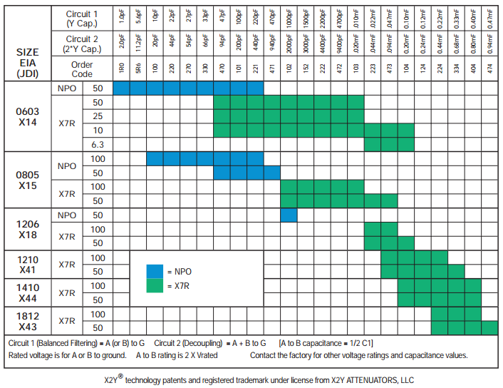
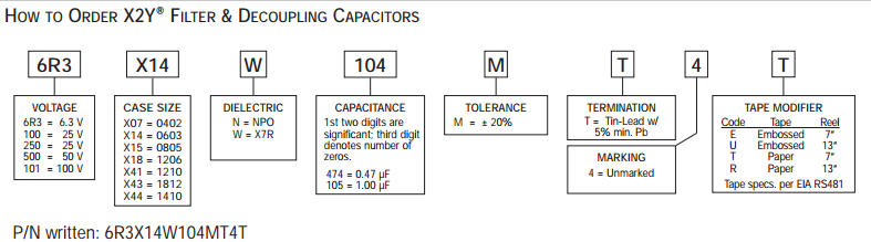
* Not all combinations create valid part numbers, ask our Apps Engineering Team for assistance creating a valid part number Request for assistance


Click below to see the new Global Part Number Reference Chart for this product

Legacy How to Order Information
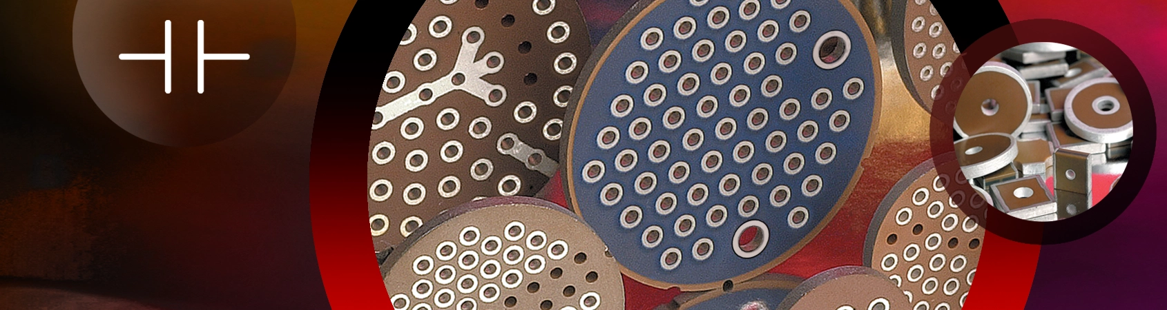
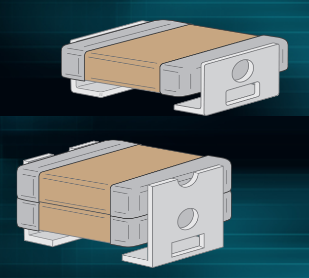
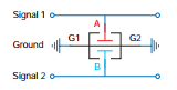
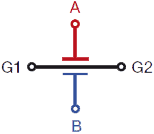
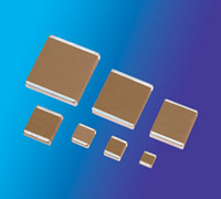
EMI filter capacitors employ a unique, patented low inductance design featuring two balanced capacitors that are immune to temperature, voltage and aging performance differences. These components offer superior decoupling and EMI filtering performance, virtually eliminate parasitics, and can replace multiple capacitors and inductors saving board space and reducing assembly costs.
Sn-Pb EMI Filter & Decoupling Capacitors

Advantages:

  • One device for EMI suppression or decoupling
  • Replace up to 7 components with one EMI
  • Differential and common mode attenuation
  • Matched capacitance line to ground, both lines
  • Low inductance due to cancellation effect

Applications:

  • Amplifier Filter & Decoupling
  • High Speed Data Filtering
  • EMC I/O Filtering
  • FPGA / ASIC / μ-P Decoupling
  • DDR Memory Decoupling

Capacitance Selection

Tin-lead EMI Capacitance chart

Electrical Characteristics

EMI Filtering Scc21

EMI Filtering Circuit S21 Signal-to-Ground circuit EMI Filtering Circuit S21 Signal-to-Ground

Power Bypass S21

EMI Decoupling Circuit S21 Power-to-Ground circuit EMI Decoupling Circuit S21 Power-to-Ground

Mechanical Specifications

Equivalent Circuits

EMI Mechanical Drawing diagramEMI Mechanical Drawing chip view

Cross Sectional View

EMI Cross Section Mechanical Drawing

Dimensional View

EMI Mechanical Schematic

Mechanical Specifications

 0402 (X07) 0603 (X14)0805 (X15)1206 (X18)1210 (X41)1410 (X44)1812 (X43)
  IN mm IN mm IN mm IN mm IN mm IN mm IN mm
L0.045 ± 0.003 1.143 ± 0.0760.064 ± 0.0051.626 ± 0.1270.080 ± 0.0082.032 ± 0.2030.124 ± 0.0103.150 ± 0.2540.125 ± 0.0103.175 ± 0.2540.140 ± 0.0103.556 ± 0.2540.174 ± 0.0104.420 ± 0.254
W 0.024 ± 0.003 0.610 ± 0.076 0.035 ± 0.005 0.889 ± 0.127 0.050 ± 0.008 1.270 ± 0.203 0.063 ± 0.010 1.600 ± 0.254 0.098 ± 0.010 2.489 ± 0.254 0.098 ± 0.010 2.490 ± 0.254 0.125 ± 0.010 3.175 ± 0.254
T 0.020 max 0.508 max0.026 max 0.660 max 0.040 max 1.016 max 0.050 max 1.270 max 0.070 max 1.778 max 0.070 max 1.778 max 00.090 max 2.286 max
EB 0.008 ± 0.003 0.203 ± 0.076 0.009 ± 0.005 0.229 ± 0.127 0.009 ± 0.004 0.229 ± 0.102 0.009 ± 0.004 0.229 ± 0.102 0.009 ± 0.005 0.229 ± 0.127 0.009 ± 0.005 0.229 ± 0.127 0.009 ± 0.005 0.229 ± 0.127
CB 0.010 ± 0.003 0.305 ± 0.076 0.0018 ± 0.005 0.457 ± 0.127 0.022 ± 0.005 0.559 ± 0.127 0.040 ± 0.005 1.016 ± 0.127 0.045 ± 0.005 1.143 ± 0.127 0.045 ± 0.005 1.143 ± 0.127 0.045 ± 0.005 1.143 ± 0.127

How to Order

Tin Lead EMi Part Number Breakdown
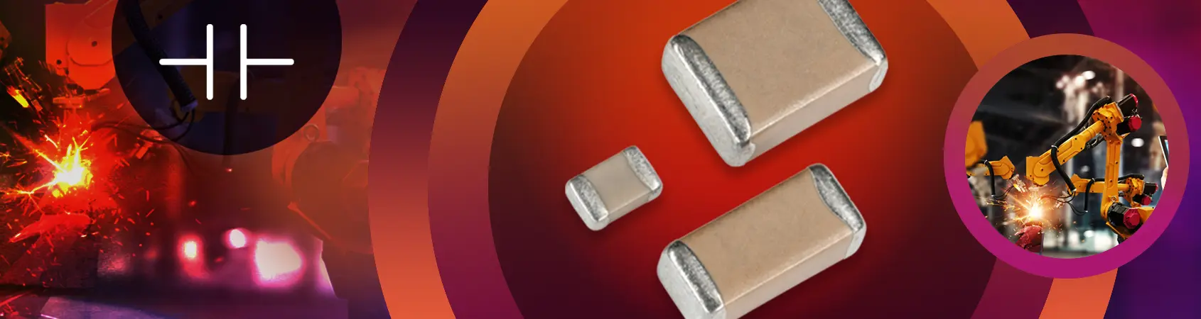
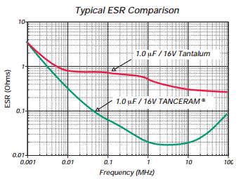
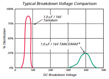
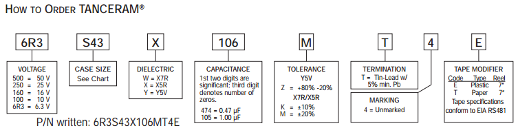
TANCERAM® chip capacitors can replace tantalum capacitors in many applications and offer several key advantages over traditional tantalums. Because Tanceram® capacitors exhibit extremely low ESR, equivalent circuit performance can often be achieved using considerably lower capacitance values. Low DC leakage reduces current drain, extending the battery life of portable products. Tancerams® high DC breakdown voltage ratings offer improved reliability and eliminate large voltage de-rating common when designing with tantalums.
Sn-Pb Large Size Capacitor Chips Tin Lead Loarge size diagram

Advantages:

  • Low ESR
  • Higher Surge Voltage
  • DReduced CHIP Size
  • Higher Insulation Resistance
  • Low DC Leakage
  • Non-polarized Devices
  • Improved Reliability
  • Higher Ripple Current

Applications:

  • Switching Power Supply Smoothing (Input/Output)
  • DC/DC Converter Smoothing (Input/Output)
  • Backlighting Inverters
  • General Digital Circuits
Tin-lead Tanceram Typical ESR Comparison
Tin-lead Tanceram Typical Breakdon Comparison

Capacitance Selection

Tin Lead Tanceram Capacitance chart

Electrical Specifications

  X7R X5R
Temperature Coefficient: ±15% (-55 to +125°C) ±15% (-55 to +85°C)
Dissipation Factor: For ≥ 50 VDC: 5% max.
For ≤ 35 VDC: 10% max.
For ≥ 50 VDC: 5% max.
For ≤ 35 VDC: 10% max
Insulation Resistance
(Min. @ 25°C, WVDC)
100 ΩF or 10 GΩ, whichever is less
Dielectric Strength: 2.5 X WVDC, 25°C, 50mA max.
Test Conditions: Capacitance values ≤ 10 µF: 1.0kHz±50Hz @ 1.0±0.2 Vrms
Capacitance values > 10 μF: 120Hz±10Hz @ 0.5V±0.1 Vrms

How to Order

Tin Lead Tanceram Part Number Breakdown