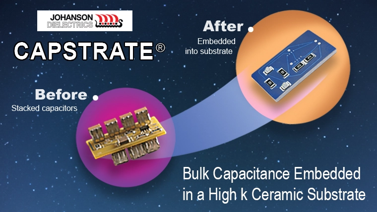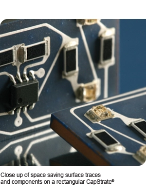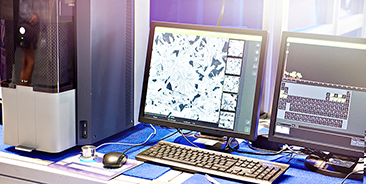
IDEAL TECHNOLOGY FOR DETONATORS
CapStrates®
- Multilayer Ceramic Substrate with Buried Capacitors
- High k ceramic material is available in NP0 or X7R
- Buried Bulk Capacitance
1 / 5
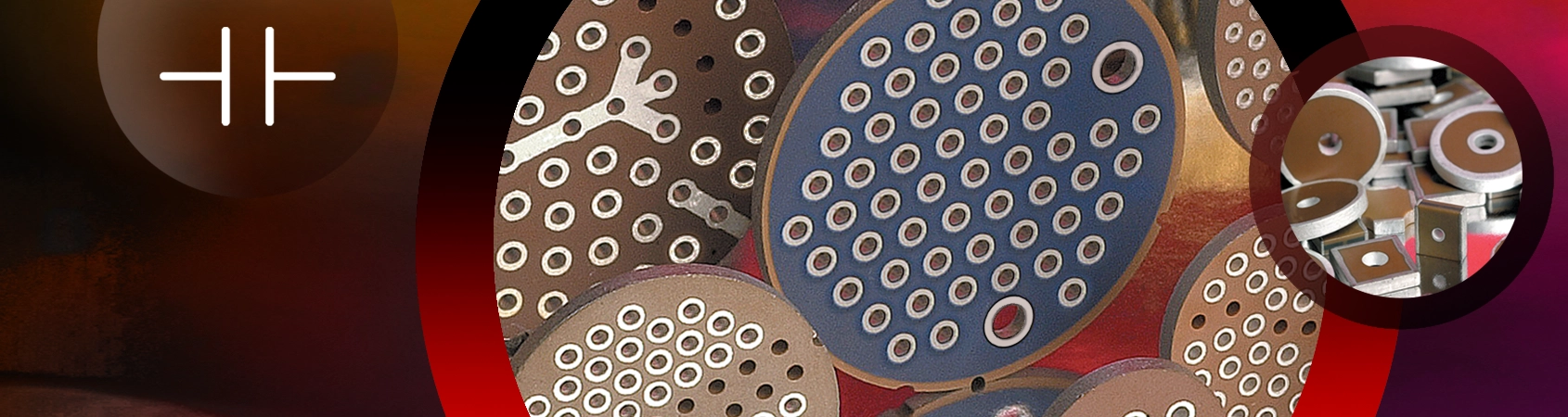
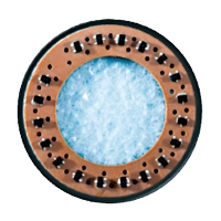
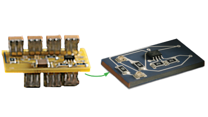
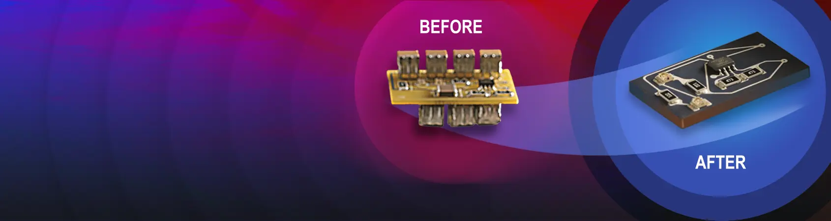
CUSTOM DESIGNS & GEOMETRIES
Planar & Discoidal Capacitors
- Circular Arrays and Rectangular Arrays
- Widely Used in EMI Filtering Systems
- Offered in NP0, X7R and MOV (Metal Oxide Varistor)
2 / 5
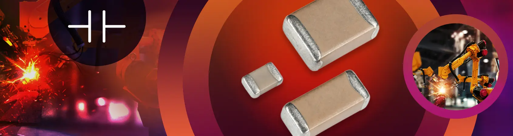
DIVERSE CASE SIZES, VOLTAGES & CAPACITANCE RANGES
High Voltage MLCC Capacitors
- Safety Capacitors Available
- DC Voltages from 500 through 6KV
- Soft Polyterm available to reduce stress
3 / 5
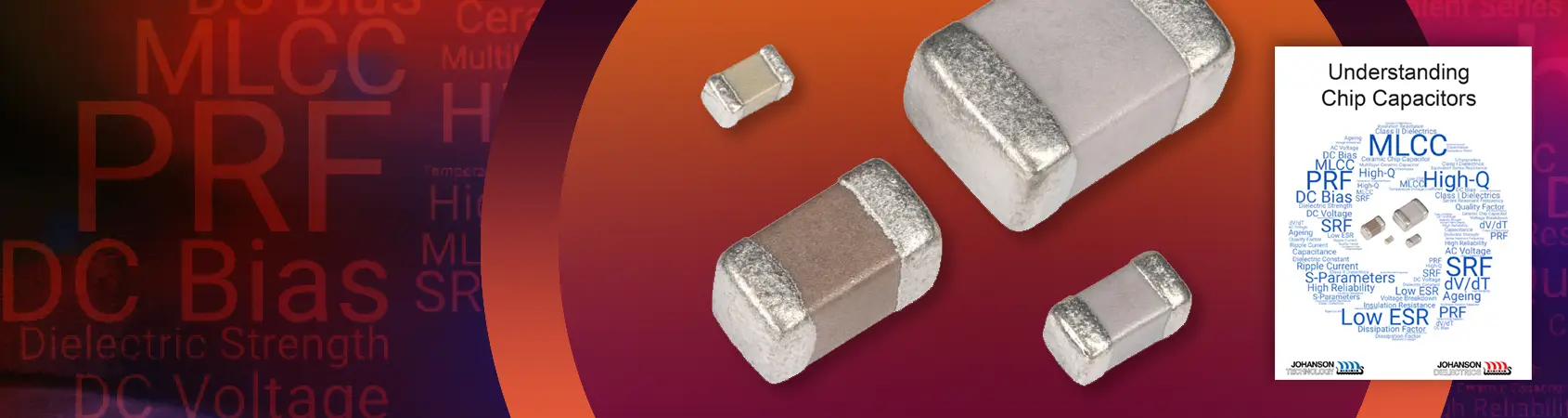
ELECTRICAL ENGINEER'S RESOURCE
Understanding Chip Capacitors
- Get basic understanding of ceramic chip capacitors
- Includes information on dielectric materials, electrical properties, testing parameters and more
4 / 5
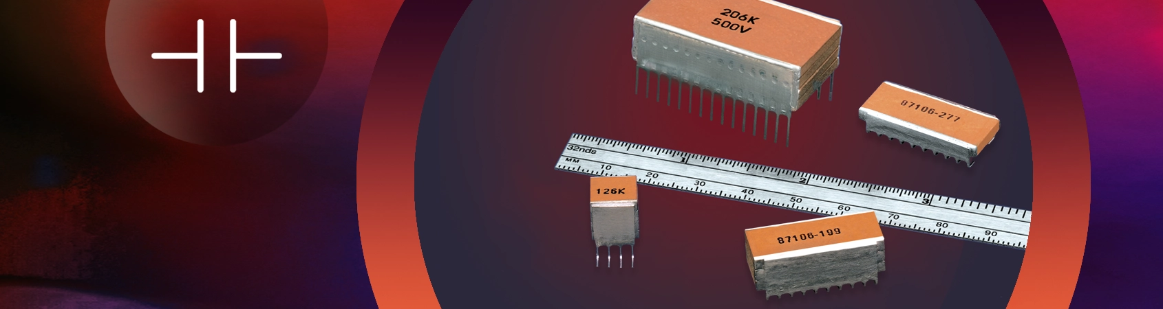
MANY SIZES, VOLTAGES & CAPACITANCE VALUES
SMPS Switchmode Capacitors
- 50 to 500 VDC Standard
- NPO & X7R Dielectrics
- Low ESR / Low ESL, Ideal for SMPS Filtering Applications
- Contact us for your unique requirements
5 / 5